3.1. Custom Configurations
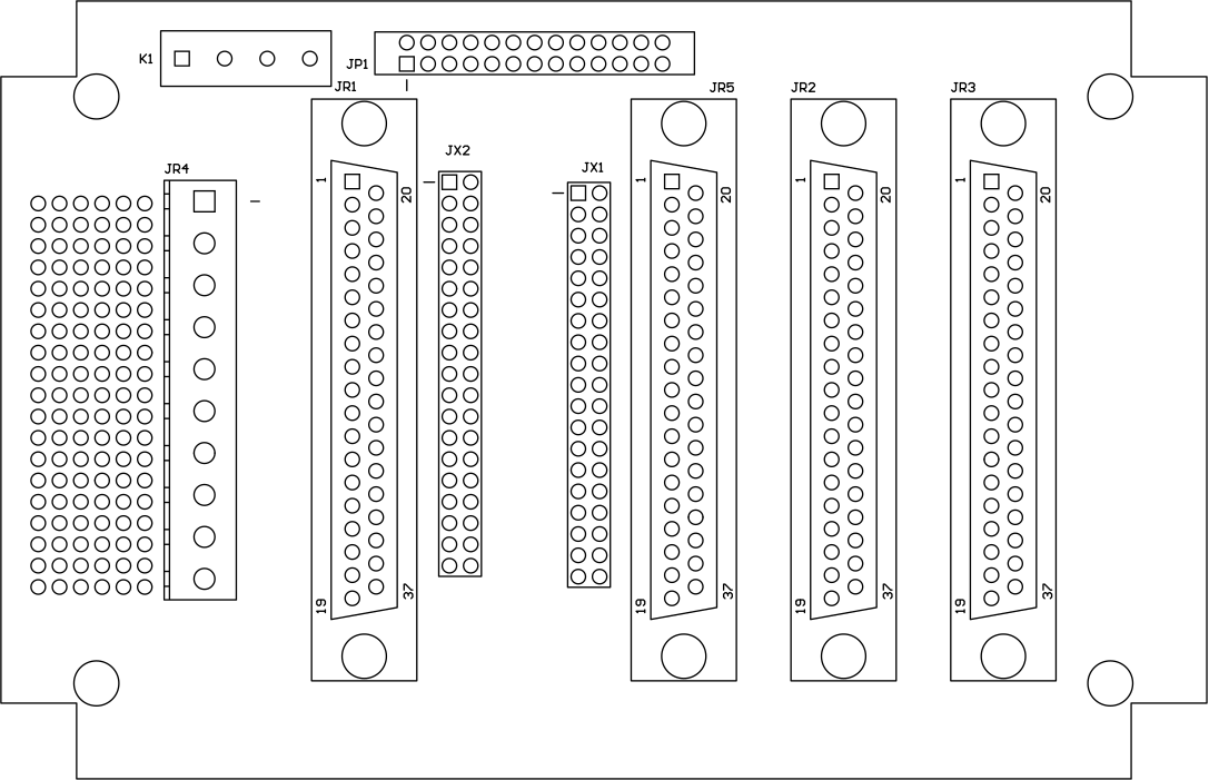
The UID permits users to design and implement their own control circuitry to control or monitor the power supply’s inputs or outputs. As shown in Fig. 3.1 and Fig. 3.2, the UID has a general purpose area on its printed circuit board to configure custom circuitry or to provide interconnections to utilize connector JR4.
3.1.1. Connector Pad Interface
Table 3.1 shows the interface of master and slave connectors JR1 through JR3 with the corresponding pad areas of JX1 and JX2. Connectors JR2 and JR3 are interconnected to allow daisy chain connections for multiple UID units.
3.1.2. User Terminal Connector (JR4)
JR4 is a 10-terminal connector that mates to a screw terminal plug. This connector is user defined and can be utilized to externally monitor or control power supply functions. Table 3.2 shows the interface of connector JR4 and the corresponding pad area, JX3. For example, connecting a wire from terminal 1 of JX3 (USER1) to terminal 15 of JX1 provides a signal to indicate the master power supply is operational.
JR4 Terminal |
JX3 Pad |
Description |
|---|---|---|
1 |
1 |
USER1 |
2 |
2 |
USER2 |
3 |
3 |
USER3 |
4 |
4 |
USER4 |
5 |
5 |
USER5 |
6 |
6 |
USER6 |
7 |
7 |
USER7 |
8 |
8 |
USER8 |
9 |
9 |
USER9 |
10 |
10 |
USER10 |
3.1.3. Multipurpose Area
The multipurpose area in the center of the printed circuit board enables the user to add circuitry within the UID. The multipurpose area provides sufficient space to add components like or’ing diodes for simultaneously monitoring two diagnostic signals. One example is to connect the anodes of two diodes to the OCT and OVT alarm signals and interconnect the cathodes. This provides a diagnostic signal on either the OCT or OVT alarm signal.
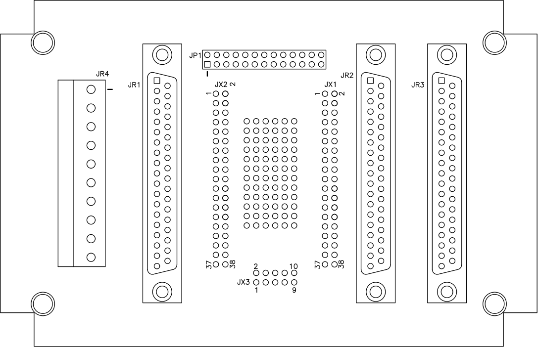
Fig. 3.1 Printed circuit board layout of the UID46 and UID47