


프로그래머블 DC 전원공급장치에 적용되는 제어 루프 변조
Introduction
Characteristics of laboratory quality, dc power supplies have changed greatly over the past two decades. Application demands have moved from the ideal voltage source with no series impedance or the ideal current source with infinite parallel impedance to user programmable output characteristics; these new applications allow for power source emulation with higher bandwidth and better response times. Box shaped voltage current profiles controlled with two knobs, fold back limiting, crowbars, and over current tripping are accepted as the most minimum requirements or they are now not needed at all.
Today, engineers demand dc power supplies with output characteristics that can be programmed for their ever-changing applications. Functional relationships between voltage and current, time dependent profiling, computer interfacing, higher bandwidth performance, safe remote sensing, and a host of programmable features, that were virtually impossible to implement without the programmability of today’s digital devices, are needed to meet today’s demands. Emphasis has changed from providing dc power with control to providing control with dc power.
The physical properties of dc power supplies have changed along with its features. Improvement in electronic switch technology and resulting increasing power processing speeds have allowed power supplies to become smaller and more responsive to load and line variations. New applications place power supplies in abusive environments: tighter packaging in equipment racks, utility trailers with poor air quality or with only water to remove semiconductor power losses, or in other locations where power supplies of the past could not effectively function.
Modulation of the Control Loop
About a decade ago, Magna-Power Electronics introduced a very basic feature in its transition from analog to embedded microprocessor-based control: modulation [1]. Modulation allows a set point adjustment of voltage or current by another input. Modulation signals can be derived from an external device, such as a thermistor, or from sampling output current or voltage. When used with software containing advanced numerical methods, feeding output voltage or current to adjust set point current or voltage allows user defined output profiles. Systems, incorporating this feature, introduce another negative feedback path with gain controlled by a user programmed attenuator.
Figure 1 illustrates a block diagram of a power supply using voltage control regulation with output current fed into the modulation input. The closed loop system is configured to regulate output voltage according to the output voltage of the D to A converter, Vx. Two inputs are fed into the A to D converter, Vref and VMOD, and the microprocessor can be programmed to produce an output voltage dependent of these two inputs. Vref is a voltage reference input and VMOD is the modulation input.

변조는 설정값에 변수를 더하거나 설정값에 변수를 곱하는 방식으로 제어 루프에 도입할 수 있습니다. 가산 함수는 직렬 및 병렬 임피던스를 도입하는 데 유용하며, 승산 함수는 전압 또는 전류 소스를 조정하는 데 유용합니다. 표 1은 네 가지 대안을 설명합니다: 전압 및 전류 제어를 위한 제어 입력 1과 2, 그리고 각각 승산 및 가산 함수를 위한 함수 유형 0과 1입니다.
| Function Type | ||
|---|---|---|
| Control Input | 0 | 1 |
| 1 | `V_o=G_v[V_("ref")*"Mod"("VMOD")]` | `V_o=G_v[V_("ref")+"Mod"("VMOD")]` |
| 2 | `I_o=G_i[I_("ref")*"Mod"("VMOD")]` | `I_o=G_i[I_("ref")+"Mod"("VMOD")]` |
Notes:
- Vo is the adjusted output voltage as a function of the modulation operator
- Io is the adjusted output current as a function of the modulation operator
- Vref is the input voltage set point reference
- Iref is the input current set point reference
- VMOD is the input modulation set point voltage
- Gv is the system gain as define by the full scale output voltage, Vofs, divided by the maximum input voltage set point reference, Vrefm
- Gi is the system gain as define by the full scale output current, Iofs, divided by the maximum input current set point reference, Irefm
Mod(VMOD), modulation, can be an expression, constant, or other numerical operator. A user-friendly method chosen by Magna-Power Electronics is a table-based algorithm using piecewise linear approximation. This numerical method allows linear or nonlinear modulation to be introduced by defining constants in a table.
Table 2 and resulting curve Figure 2 illustrate a simple example of Function Type 0 modulation as applied to a 100 V, 150 A power supply. In this example and the one illustrated in Figure 1, the power supply is programmed to produce a constant power output. Current, Io, is used as the programming operator for Mod. The method requires Io to be monitored and applied to the programming or modulation input, VMOD. As illustrated, VMOD is set to linearly respond to current.
where:
- Vrefm: full scale input voltage set point reference
- Rx: transresistance of the current transducer
| Row | VMOD (Vdc) | Mod | Vo (Vdc) | Io (Adc) | Po (W) |
|---|---|---|---|---|---|
| 1 | 2.50 | 1.000 | 100.00 | 37.50 | 3750.00 |
| 2 | 2.94 | 0.850 | 85.00 | 44.12 | 3750.00 |
| 3 | 3.57 | 0.700 | 70.00 | 53.57 | 3750.00 |
| 4 | 4.55 | 0.550 | 55.00 | 68.18 | 3750.00 |
| 5 | 6.25 | 0.400 | 40.00 | 93.75 | 3750.00 |
| 6 | 10.00 | 0.250 | 25.00 | 150.00 | 3750.00 |
Piecewise linear approximation makes a continuous curve by interpolating points on the curve between those programmed. For example, Vo is 77.5 Vdc if the operating current is 48.85 Adc. Accuracy of the approximation improves with more data points.
Challenges of Control Loop Modulation
Hardware Constraints
Modulation, as described above or by other similar means, allows emulation of power sources such as photovoltaic cells, batteries, and fuel cells. The dynamics of these applications require a frequency response beyond that needed by conventional power supplies. Furthermore, the embedded firmware must be capable of handling the speed of the application. Together, a power supply designed to perform with high speed modulation will have different characteristics than conventional power supplies.

A power supply designed to utilize modulation must have higher bandwidths and tolerate higher slew rates; such power supplies must incorporate higher bandwidth output filters. Output filters are required to filter unwanted ac components produced in the power conversion process, but with modulation or with other superimposed ac source generation, signals beyond dc must be allowed to pass through the output terminals of the power supply. Higher bandpass filters are required for such applications and they must be designed to separate wanted and unwanted power components. Higher bandwidth power supplies generally have increased output voltage ripple. Increasing the switching frequency of the power supply helps accomplish both goals, but at the cost of increased switching loss.
In conventional applications, high-capacitance, low ESR, aluminum electrolytic capacitors are the conventional components used at the output terminals; these components provide a shunt path for high-frequency harmonic currents. In higher bandwidth and high slew rate applications, these components are subjected to greater voltage deviations requiring higher power processing demands during charge and discharge periods. Furthermore, the reliability of aluminum electrolytic capacitors is greatly influenced by subjected ac currents. Lower capacitance, high-performance film capacitors must be deployed to circumvent these issues.
Higher bandwidth and high-slew rate operation also place higher demands on protection of power semiconductor components. Simple over current trip protection circuits are not suitable for this application because the power supply must tolerate these rapid output changes. To the power processing semiconductors, the load is both internal and external to the power supply. The current required to charge and discharge the output filter and external load capacitors must be taken into consideration. Slew-rate must be limited to protect power processing semiconductors.
Software Constraints
Introduction of modulation complicates the power supply’s control loop. Normally, one parameter, output voltage or output current, is compared against a reference and is adjusted to maintain an operating point close to the reference. As shown in Figure 1, the system requires an error amplifier and circuitry for closed loop compensation. If the gain of the amplifier is too high or if the compensation is not properly designed, the power supply will become unstable and oscillate.
Modulation adds a second parameter and an inherent lagging response. At a specific operating point, the programming parameters need to be analyzed digitally and applied to the modulation input. Using fast digital signal processors, DSP’s, is required to minimize delays and make calculations of these devices transparent.
Modulation can be programmed with gains of different magnitudes. The gain for modulation can be defined as the change in Mod between two rows of a table and will have stability issues similar to the closed loop error amplifier. Forcing the power supply output to make large changes between two operating points can cause an unstable response. Slew rate limiting is an effective means for getting around these constraints, but slew rating limiting has a negative effect on the speed of response or the bandwidth of the system.
Leadless Remote Sensing
Positive Slope, Leadless Remote Sensing
Remote sensing is used to improve the degradation of regulation which will occur at the load when the voltage drop in the connecting wires is appreciable. Normally, this feature is accomplished through the connection of sense leads connected directly to the load rather than to the output terminals of the power supply. With these connections, the leads between the source and load are placed within the control loop and the resulting voltage drop will be corrected along with other parameters. The power supply must have sufficient output voltage to support the output voltage plus the lead voltage within specified tolerance.
Sometimes sensing the load voltage is not practical or possible. Long tethers, requiring heavy cables, are hard to fabricate with sense lead cables. Sensing output current and raising the power supply’s output voltage can be an effective alternative to adding remote sense leads. While this might seem trivial for relatively short lead lengths, it is not for applications of distant load points such as ocean tethers to vehicles.
Figure 3 illustrates a dc power supply with lead and load resistance. The load voltage, Vload, can be expressed as:
where:
- Vo: power supply output voltage
- Io: power supply output current
- Rlead: lead resistance between the power supply and load

그림 1에 설명된 제어 방식을 적용하여 출력 전류를 변조 입력에 인가하고, 식 (6)의 Vo를 제어 입력 1, 함수 유형 1 변조(표 1 참조)로 대체하면, Vload는 다음과 같습니다:
조건:
In this example, the power supply’s output voltage adjusts in response to output current compensating for the voltage drop caused in the connecting leads to the load.
Negative Slope, Leadless Current Sharing
There are many schemes for sharing current when multiple power supplies are connected in parallel. Most of them require some form of communications between the multiple power supplies to share output current information. Generally, this is done by designating one power supply as the master and the others as slaves. The master power supply is operated in voltage mode control and the slave power supplies are operated in current mode control. The set point current for the slave power supplies is provided by the master. The drawback of this approach is that the system is totally dependent upon operation of the master and malfunction of the master power supply means malfunction of the system.
For systems requiring N+1 redundancy, or systems requiring excess capacity of one power supply in the event of one failure, master/slave parallel operation is not well suited. For these applications, all parallel connected power supplies must be totally independent. Connecting power supplies in parallel and allowing automatic crossover between voltage mode and current mode control will work, but current sharing will not be equal. A preferred approach, as illustrated in Figure 4, is to introduce a small series resistance on each of the parallel connected power supplies to ballast the load between the other supplies. The resistance, or in this case pseudo resistance, can be introduced without additional losses by utilizing Control Input 1, Function Type 1 modulation (see Table 1). Ideally, programming both of the paralleled connected power supplies the same, the output voltage, Vload, can be made to represent:
또는 출력 전류로 표현하면
where:
- Vo1, Vo2: power supply output voltage without source resistance
- Io1, Io2: power supply output current
- Ro: output source resistance
For this application, the source resistance requires a negative slope.

Power Source Emulation
Battery Emulation
The impedance and cell voltage of batteries and battery packs vary according to a number of factors, such as, but not limited to, chemistry, mechanical construction, the number of charge/discharge cycles, temperature, and depth of discharge. These variables can be defined with voltage and current profiles and applied to the modulation input of a dc power supply. One modulation table cannot completely emulate a battery since the profile changes with multiple variables: primarily with depth of discharge and temperature of operation. Therefore, multiple tables are required to address the different variables and need to be integrated into the control algorithm. Detection of both voltage and current over a period of time provides the parameters needed to calculate depth of discharge. Further tables are required to adjust these profiles with temperature. At specific increments of time and temperature, modulation tables need to be replaced. Control Input 1, Function Type 0 modulation is best suited for this application.
Quickly loading tables in anticipation of the next operating point presents itself as a software challenge. Magna-Power Electronics uses cache tables embedded in storage to quickly move from one table to another.
Solar Emulation
Photovoltaic arrays produce non-linear voltage and current characteristics that are a function of temperature, irradiance, and several other technology-dependent variables. Devices interfacing to photovoltaic arrays, such as inverters and DC-DC converters, set an operating point near the array’s maximum power output: a process called maximum power point tracking. A DC power supply capable of emulating these non-linear characteristics provides user defined methods for development and evaluation of photovoltaic connected devices.
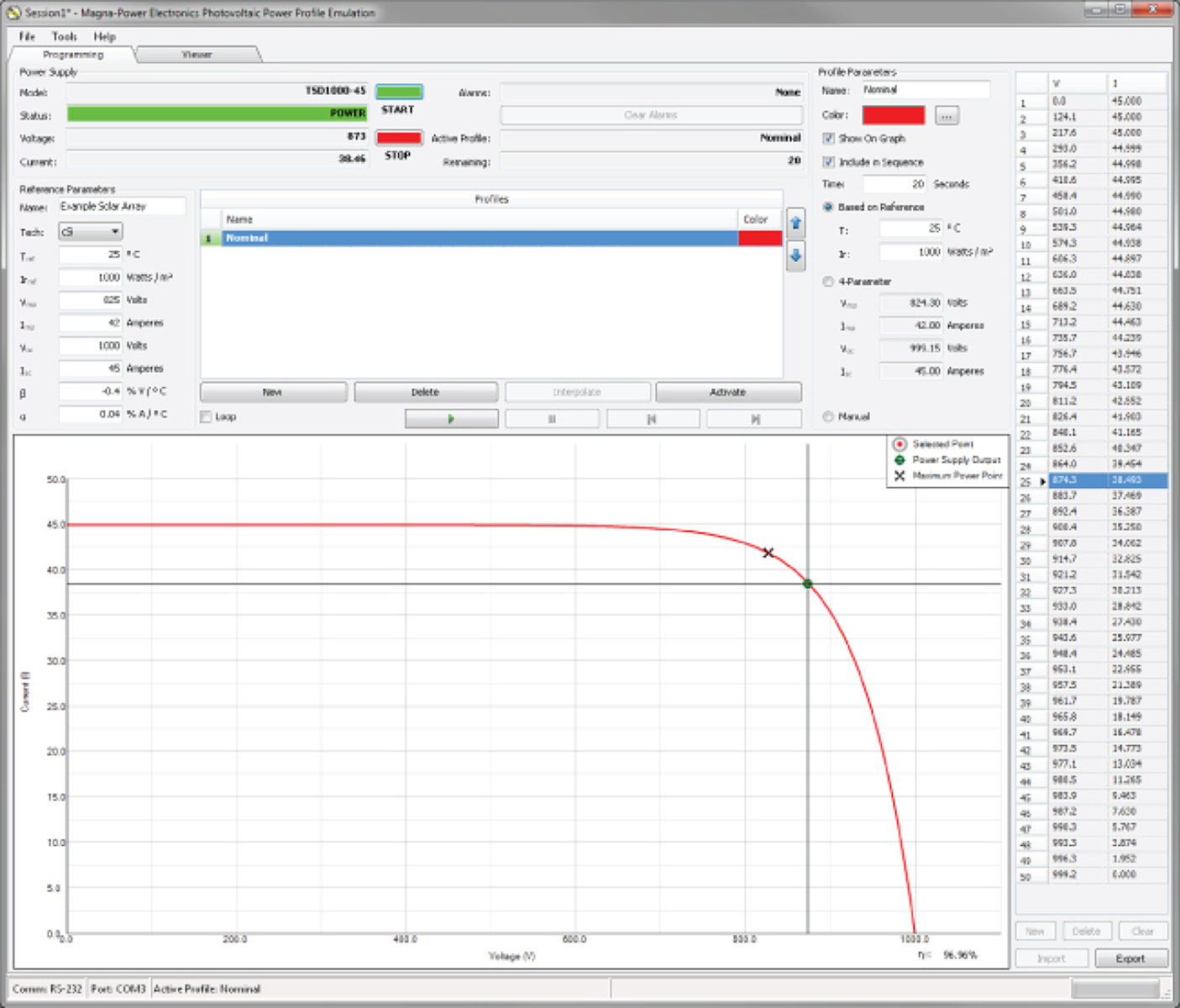
Magna-Power Electronics’ modulation feature can be used to define a 50-point photovoltaic profile at distinct temperature and irradiance values within the memory of the power supply. The power supply performs piece-wise-linear approximation between points to ensure high resolution operation. Data is loaded into the power supply’s memory using an external program, Photovoltaic Power Profile Emulation, PPPE, that was developed specifically for the application. It defines more points near the curve’s most non-linear region—the curve’s knee—for the highest fidelity. PPPE software uses an EN50530 model to define a continuous voltage-current profile with temperature and irradiance dependencies. The model enables emulation of thin-film, poly-crystalline, mono-crystalline, or custom user-defined photovoltaic technologies. Timing constraints for updating voltage and current profiles are minimized by sequentially and continuously sending data to the power supply’s cache table and swapping data when needed for the next update.
Both Control Input 1, Function Type 0 (voltage control) or Control Input 2, Function Type 0 (current control) modulation are applicable for this application. The load’s control mode and method of operation determine the best method of modulation. Table 3 provides an example of an emulated photovoltaic array profile for a 1000 Vdc, 45 Adc, Magna-Power Electronics TSD1000-45 power supply. For simplicity, the example is reduced to only 10 points. The corresponding curve, implemented with PPPE software, is shown in Figure 5.
| Entry | Voltage (Vdc) | Current (Adc) | VMOD | Mod |
|---|---|---|---|---|
| 1 | 0.00 | 45.00 | 9.992 | 0.050 |
| 2 | 293.00 | 44.99 | 9.903 | 0.128 |
| 3 | 574.30 | 44.94 | 9.697 | 0.366 |
| 4 | 689.20 | 44.63 | 9.531 | 0.510 |
| 5 | 794.50 | 43.11 | 9.273 | 0.671 |
| 6 | 840.10 | 41.17 | 9.078 | 0.757 |
| 7 | 892.40 | 36.39 | 8.640 | 0.877 |
| 8 | 907.80 | 34.06 | 8.401 | 0.915 |
| 9 | 977.10 | 13.03 | 5.010 | 1.000 |
| 10 | 1000.00 | 0.00 | 0.000 | 1.000 |
References
- Operating and Service Manual TS Series IV DC Power Supplies, Magna-Power Electronics, Flemington, NJ, May. 2013.