




SiC 및 GaN 이중 펄스 테스트: 고전압 DC 버스 전원 공급 장치
SiC 및 GaN 광대역갭 반도체의 이중 펄스 테스트(DPT)를 위한 DC 전원 공급 장치 선정 가이드로, 전압, 전류, 프로그래밍 기능 및 안전 요구 사항에 대한 실제 적용 예제와 지침을 제공합니다.
From Curve Tracers to Nanosecond Transitions
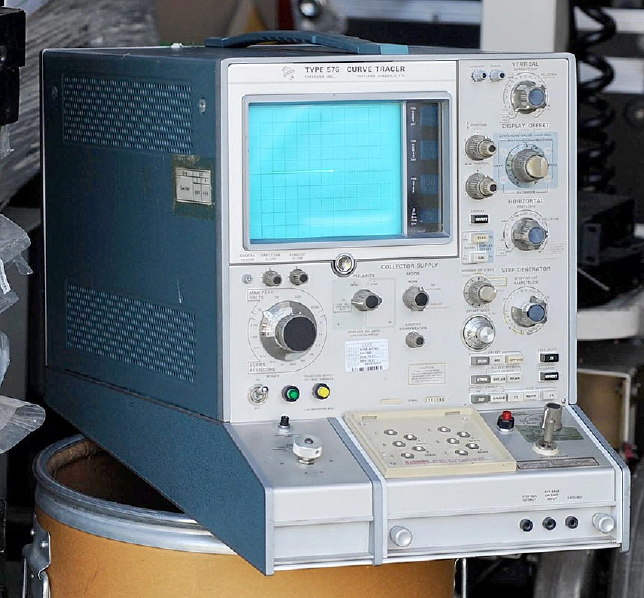
For most of the history of power semiconductor characterization, the workhorse instrument sat quietly in the corner of the lab: the curve tracer. Tektronix introduced the first commercial curve tracer in 1955, and the legendary Type 576, introduced in 1969 and capable of sweeping 1500 volts and 20 amperes through a device under, defined how a generation of power engineers understood transistors, diodes, thyristors, and IGBTs. The 576 and its successors, the 370A/B series, remained in production into the mid-1980s and are still in active use today for failure analysis and teaching.
Curve tracers are fundamentally steady-state instruments. They sweep a voltage, measure the resulting current, and plot the I-V characteristic on a screen. For silicon MOSFETs and IGBTs switching at tens of kilohertz in yesterday’s power electronics, that was enough.
That era ended with the commercial emergence of silicon carbide (SiC) and gallium nitride (GaN) power devices. Wide bandgap (WBG) semiconductors switch at rates that turn switching loss into the dominant loss mechanism. The parameters that determine system efficiency — turn-on energy (Eon), turn-off energy (Eoff), reverse recovery energy (Err), voltage overshoot, dv/dt, di/dt — live entirely in the dynamic behavior of the device during nanosecond transitions. A curve tracer cannot see them.
The industry’s answer is the Double Pulse Test (DPT), codified in JEDEC JEP182 and the IEC 60747-8/-9 standards. DPT is now a required step in datasheet generation, converter design validation, and production-line characterization at every serious power semiconductor manufacturer.
This application note covers the fundamentals of DPT briefly, then focuses on the element most often glossed over in DPT discussions: the DC bus supply that anchors every setup, and the specific engineering decisions that go into selecting one correctly.
What DPT Measures
A double pulse test extracts the dynamic switching parameters that datasheets rely on and converter designs depend on:
- Turn-on: turn-on delay (td,on), rise time (tr), turn-on energy (Eon), dv/dt, di/dt
- Turn-off: turn-off delay (td,off), fall time (tf), turn-off energy (Eoff), dv/dt, di/dt
- Reverse recovery (of the freewheeling device): reverse recovery time (trr), peak reverse recovery current (Irr), reverse recovery charge (Qrr), reverse recovery energy (Err)
These parameters feed directly into converter efficiency calculations, thermal modeling, EMI prediction, and gate drive optimization, which is why every WBG device datasheet publishes them, and why every converter designer wants to verify them on the specific parts they’re buying.
How Double Pulse Testing Works
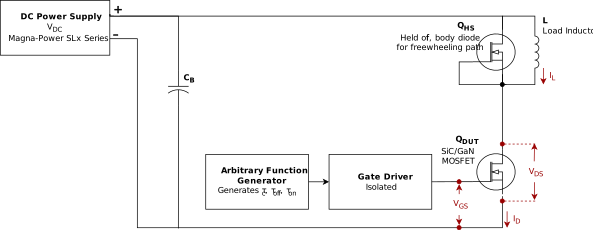
The canonical DPT circuit is a half-bridge with an inductive load. The device under test is typically the low-side switch. The high-side device, often another MOSFET with its body diode, or a dedicated freewheeling diode, provides the current path during the freewheeling interval. A large DC-link capacitor bank supplies the pulsed energy, and a DC power supply charges the bank to the test voltage.
The three phases
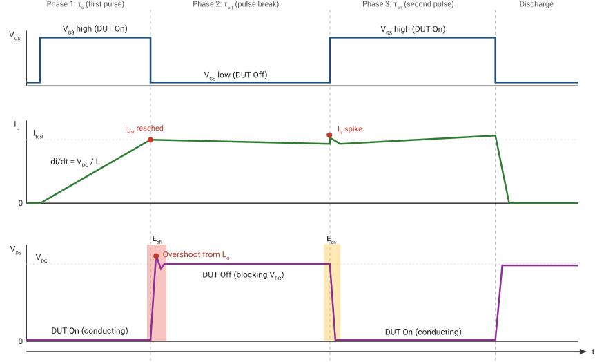
A double pulse test, despite its name, has three distinct intervals.
Phase 1: Charging pulse (τc)
The DUT turns on. Current ramps up linearly in the load inductor according to:
세 가지 단계
이중 펄스 테스트는 그 명칭과 달리 세 가지 구별되는 구간으로 구성됩니다.
1단계: 충전 펄스 (τc)
DUT가 턴온됩니다. 부하 인덕터의 전류가 다음 식에 따라 선형으로 증가합니다:
첫 번째 펄스 폭 τc는 목표 시험 전류 Itest에 도달하도록 설정됩니다:
At the end of this interval, the DUT turns off. This is where the first turn-off event is captured — at the target test current, with the DC bus fully charged. This is the Eoff measurement.
Phase 2: Pulse break (τoff)
The DUT is off. Inductor current circulates through the high-side freewheeling device. This interval must be long enough for switching transients to fully decay, but short enough that inductor current doesn’t drop significantly.
Phase 3 Second pulse (τon)
The DUT turns on again. Now the turn-on event is captured at the target current, with realistic di/dt conditions. Simultaneously, the freewheeling device undergoes reverse recovery, which is captured as the peak Irr spike. This is where Eon and Err are measured.
스위칭 손실 및 커패시터 뱅크 설계
스위칭 손실은 전환 구간에서 순시 전압과 전류의 곱을 적분하여 계산합니다. 턴온 시:
Eoff and Err follow the same form over their respective intervals. Integration limits are defined by JEDEC JEP182, typically at 10% voltage and current crossing thresholds. Modern oscilloscopes with DPT application software automate the calculation.
The DC-link capacitor bank must be large enough that the bus voltage stays substantially constant during the pulse. From energy balance, with small allowable droop ΔVDC:
실용적인 DPT 설정은 수십에서 수천 마이크로패럿의 병렬 필름 커패시턴스를 사용하며, 등가 직렬 인덕턴스를 최소화하도록 배치합니다. 이 커패시터 뱅크 크기 산정 방정식은 전원 공급 장치 선정 계산의 입력값이 되기도 합니다.
상용 시장 현황: DPT 벤치 구축을 위한 세 가지 접근 방식
업계에서는 크게 세 가지 범주의 DPT 설정으로 수렴하고 있습니다.
턴키 시스템
게이트 드라이브, 픽스처, 측정 장비, 분석 소프트웨어, 그리고 경우에 따라 DC 버스 전원까지 포함된 완전 통합형 공급업체 패키지입니다. 예시: Keysight PD1500A, Rohde & Schwarz + PE-Systems(R&S MXO 오실로스코프 포함). 빠른 결과 도출과 즉시 사용 가능한 JEDEC 규격 준수가 장점이지만, 전압 및 전류 범위가 고정되어 있으며 초기 투자 비용이 높습니다.
계측기 패키지
고대역폭 오실로스코프에 임의 파형 발생기, 전용 프로브, DPT 소프트웨어 옵션을 조합한 구성입니다. Tektronix의 4/5/6 Series B MSO와 WBG-DPT 애플리케이션 및 AFG31000 조합이 대표적인 예이며, 광 절연 프로브를 사용하는 Teledyne LeCroy도 또 다른 사례입니다. 턴키 시스템보다 비용이 낮고 계측기를 다른 용도로 활용할 수 있지만, 픽스처, 게이트 드라이버, 커패시터 뱅크, 부하 인덕터, DC 전원은 사용자가 직접 준비해야 합니다.
맞춤형 / DIY 테스트 벤치
반도체 제조업체, 연구소, 그리고 소자의 전압 및 전류 한계를 넓히는 OEM에서 주로 사용하는 방식입니다. 목표 시험 범위에 맞춰 모든 구성 요소를 개별적으로 선정합니다. 1700 V 이상의 소자, 대전류 모듈(수백 암페어~킬로암페어), 시험 조건이 아직 표준화되지 않은 신규 소자 구조에 대해서는 이 방식이 유일한 선택지입니다.
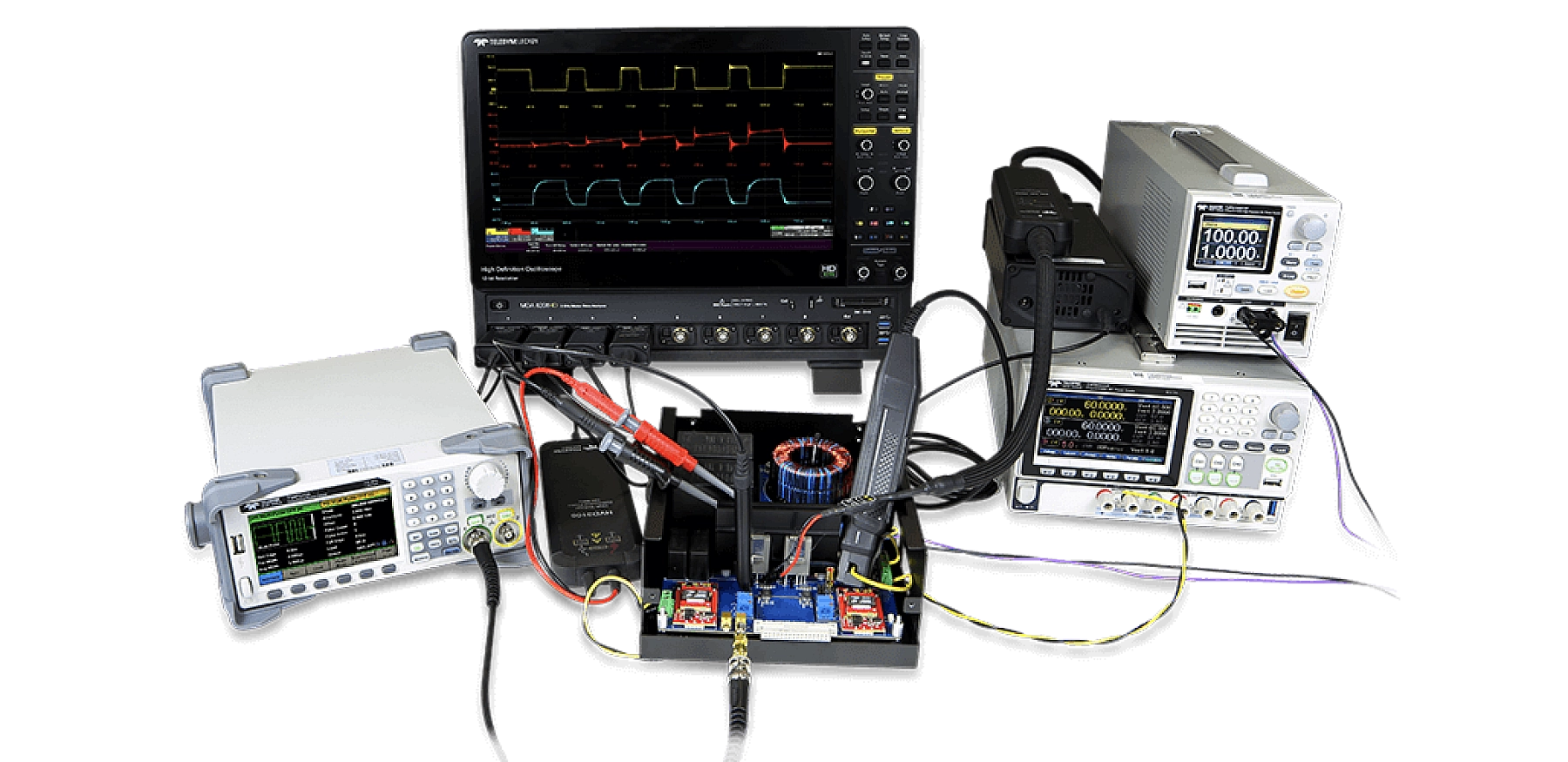
The constant across all three architectures is the DC bus supply. Every system treats it as a given. The rest of this application note covers what it actually takes to specify one correctly.
Power Supply Selection for DPT
The DC power supply in a DPT bench performs a specific and often misunderstood role. It does not source the pulsed current into the DUT directly, that energy comes from the DC-link capacitor bank. The supply’s job is to charge the capacitor bank to the test voltage and recharge it between shots, while doing so accurately, repeatably, safely, and under automated control.
That role carries specific requirements.
Voltage rating
The supply must deliver the DC bus voltage at which characterization is performed. Good practice tests WBG devices at 50–80% of their rated VDS. Practical implications:
| Device rating | Typical DPT bus voltage | Supply rating |
|---|---|---|
| 650 V GaN e-HEMT | 400 V | 500 V minimum |
| 1200 V SiC MOSFET | 800–1000 V | 1000–1500 V |
| 1700 V SiC MOSFET | 1200–1400 V | 1500–2000 V |
| 3300 V SiC module | 2500–2800 V | 3000 V+ |
| 6500 V SiC / high-V devices | 5000+ V | 6000–10000 V |
The trend line is unambiguous: device voltages are climbing. A DPT bench built around a 1500 V supply in 2020 cannot characterize the 3300 V devices entering volume production now.
Current capability and how to size it
This is where DC supply selection is most often misunderstood. The peak pulsed current flowing into the DUT during the test is sourced by the capacitor bank, not the supply. The supply’s job is to replenish the energy drawn from the capacitor bank between shots, equating to a much smaller current requirement for the supply than the peak pulse current.
There are two constraints to evaluate. The binding requirement is whichever is larger.
Energy balance (usually dominant). Each DPT shot transfers energy from the capacitor bank into the load inductor:
fshot 속도로 펄스를 반복하는 경우, 전원 공급 장치가 공급해야 하는 평균 전력은 다음과 같습니다:
최소 공급 전류는 평균 전력을 버스 전압으로 나눈 값입니다:
재충전 시간 제약 조건(높은 펄스 반복률에서 구속 조건이 됨). 커패시터 뱅크는 각 펄스 동안 ΔQ = CB · ΔVDC만큼 전하를 잃습니다. 전원 공급 장치는 가용 재충전 시간 Trecharge(일반적으로 펄스 간격에서 펄스 지속 시간과 측정 안정화 시간을 뺀 값) 내에 이 전하를 보충해야 합니다:
For most laboratory characterization work, the energy-balance equation governs. For high-throughput production parametric testing, where shots are spaced milliseconds apart and capacitor banks are sized large for high test currents, the recharge constraint dominates. Calculate both and size the supply for the larger.
Example 1: 1200 V SiC MOSFET lab characterization
A typical research lab DPT setup:
Example 2: Production-line parametric testing
여기서 재충전 제약 조건은 에너지 균형을 두 자릿수 이상 초과하며, 1000 V에서 최소 3 A(3 kW) 정격의 전원 공급 장치가 필요합니다.
실용적 시사점
대다수의 DPT 응용 분야에서 전원 공급 장치의 평균 전류 정격은 DUT의 피크 펄스 전류보다 1~3자릿수 낮습니다. 피크 DUT 전류에 맞춰 전원 공급 장치를 선정하는 것은 랙 공간과 예산을 낭비하는 과도한 사양 선정이며 실질적인 이점이 없습니다. 위의 두 가지 방정식을 사용하여 전원 공급 장치를 올바르게 선정하면, 일반적으로 훨씬 소형의 컴팩트한 전원 공급 장치로도 충분히 대응할 수 있음을 알 수 있습니다.
이 부분은 Magna-Power의 응용 엔지니어링 팀이 직접 지원하는 영역입니다. 저희는 단발 펄스 대학 연구 설비부터 고처리량 양산 파라메트릭 테스트 셀에 이르기까지 다양한 DPT 벤치용 DC 전원 공급 장치를 선정해 왔으며, 특정 구성에 대한 계산을 함께 검토해 드리겠습니다.
DPT를 위한 주요 전원 공급 장치 기능
기본적인 전압 및 전류 정격 외에도, DPT 벤치는 전원 공급 장치의 제어, 보호 및 물리적 설치 면적에 대해 특정 요구 사항을 부과합니다. 아래 섹션에서는 DPT 설비가 DC 버스 전원 공급 장치에 요구하는 구체적인 사항과 함께, 대학 연구실부터 반도체 양산 현장까지 더블 펄스 테스트의 핵심 장비로 오랫동안 활용되어 온 Magna-Power의 SLx 시리즈 및 XR 시리즈의 해당 기능을 설명합니다.
프로그래밍, 측정 및 자동화
스위칭 손실은 VDC, Itest, Tj 및 게이트 드라이브 조건에 따라 달라지므로, 다수의 버스 전압에 걸친 파라메트릭 스윕은 WBG 특성 평가에서 일상적으로 수행됩니다. 전원 공급 장치는 단순한 정적 전원이 아니라 측정 체인의 계측기이며, 깔끔하게 프로그래밍되고, 정확하게 측정하고, 시퀀서 제어에 응답하며, 연구실이 운영하는 자동화 인프라와 통합되어야 합니다.
버스 전압 설정값은 궁극적으로 DPT 측정이 디바이스의 V-I 특성 곡선 어디에 위치할지를 결정하며, 전원 공급 장치의 전압 리드백은 스위칭 손실 계산에 직접 반영됩니다. SLx 시리즈는 프로그래밍 정확도가 풀스케일 대비 최소 ± 0.06%이며, 측정 정확도가 충분히 높아 일반적인 WBG 디바이스의 측정 버짓에서 전원 공급 장치에 의한 불확도가 지배적이지 않습니다.
Parametric DPT characterization typically sweeps across multiple bus voltages per device, for example 400 V, 600 V, 800 V, 1000 V for a 1200 V SiC MOSFET, with DPT shots repeated at each setpoint. The supply has to move between setpoints cleanly and quickly. MagnaLINK distributed DSP digital control on the SLx Series implements programmable slew rates and fast programmable ramping with field-tunable gains across a wide range of load conditions, letting an automated sweep sequencer step through a full voltage-current-temperature matrix.
Digital commands over a network interface has inherent latency typically milliseconds, which can introduce jitter into tightly-coordinated DPT sequences. For applications where the supply's state needs to synchronize with the gate driver, AFG, and oscilloscope without going through the command layer, the SLx and Series provides a standard D-Sub User I/O with analog and digital logic. This I/O provides a hardware path for real-time feedback and control that's independent of the software command interface, allowing the supply can be wired directly into the test bench's interlock system, trigger logic, and analog measurement paths.
Automation infrastructure varies widely across the DPT customer base, including LabVIEW, Python over Ethernet, IVI drivers in TestStand, production floors running PLC controlled sequencers. The supply needs to integrate with whichever infrastructure is already in place, not force a change in it.
The SLx Series comes standard with dual USB (front and rear) and RS-485, with full SCPI and Modbus command-set support. Optional LXI TCP/IP Ethernet (+LXI) provides standard lab network control, and for environments running industrial automation, SLx additionally offers CANopen, EtherCAT, EtherNet/IP, ModbusTCP, and PROFINET as fully-integrated communication options, each with full command-set support, enabling direct control from industrial PLCs (Siemens PROFINET being particularly common in semiconductor fabs and automotive test cells). The XR Series comes standard with serial RS-232 and supports LXI TCP/IP Ethernet (+LXI) and IEEE-488 GPIB (+GPIB) as optional interfaces for broader lab instrumentation integration. National Instruments LabVIEW and IVI drivers are included with every supply.
Starting from Python–what Magna-Power uses in-house for its own test software–is straightforward the supply listens on a socket, SCPI commands are ASCII text, and a full DPT sweep scaffolding with logging takes a dozen lines:
import socket, time

# Connect to supply at lab network address, default SCPI socket port
s = socket.socket(socket.AF_INET, socket.SOCK_STREAM)
s.connect(('192.168.0.86', 50505))

# Identify and configure for remote control
s.sendall(b'*IDN?\n')
print(s.recv(4096).decode())
s.sendall(b'CONF:SOUR 0\n')

# Sweep across bus voltages for parametric DPT characterization
for v_bus in [400, 600, 800, 1000]:
    s.sendall(f'VOLT {v_bus}\n'.encode())
    s.sendall(b'OUTP:START\n')
    time.sleep(0.1)   # settle time before DPT shot
    # [trigger AFG, capture scope waveforms, calculate E_on/E_off]
    s.sendall(b'MEAS:ALL?\n')
    curr, volt, pwr = s.recv(4096).decode().split(',')
    print(f'V_bus={v_bus}: measured {float(volt):.2f} V, {float(curr):.3f} A')

s.sendall(b'OUTP:STOP\n')
s.close()
Self-protecting topology under load faults
DPT is inherently destructive testing. Devices routinely fail, and when they do, they typically short. The supply must respond to a load fault without cascading into supply damage, without injecting large reverse currents back into the capacitor bank, and without releasing stored energy in ways that propagate damage through the bench.
Every MagnaDC power supply supply is built on Magna-Power's signature current-fed power processing topology, which adds a control stage over conventional voltage-fed designs. Under fault conditions, this topology inherently limits fault energy: no fast-rising current spikes, no magnetic core saturation, and self-protecting behavior under short-circuit loads. For DPT applications, this is the first line of defense when a DUT fails: the power supply architecture itself resists the fault, rather than relying on firmware-controlled trip responses. Combined with the safety protections in the following section, the SLx Series and XR Series tolerate repeated DUT-failure events without taking the bench down.
Safety protections
DPT pushes devices to failure by design. A well-designed supply provides multiple layers of protection that together shield the supply, the bench, and the operator from the range of things that can go wrong, DUT shorts, runaway currents, overvoltage transients from the cap bank, thermal excursions, enclosure breaches, and operator errors. The protection strategy is layered rather than single-point: each mechanism operates independently, so no single failure defeats the whole system.
Programmable overvoltage trip (OVT) and overcurrent trip (OCT) are the first programmable layer. Both SLx Series and XR Series supplies provide OVT and OCT settings configurable from the front panel, User I/O, or via command interface, with trip thresholds independent of the output regulation setpoint. For DPT, OCT is typically set a modest margin above the expected recharge current so that any anomalous load behavior.
For thermal protection, distributed thermal switches monitor multiple points inside the supply, and control-integrity diagnostics watch the programming line, remote sense leads, and internal references. A fault on any of these conditions trips the supply independently of the programmable OVT/OCT settings.
A dedicated Interlock hardware input that inhibits the output when a contact loop is broken with a latching fault. The Interlock typically integrated with the test enclosure: a 5V-referenced dry-contact loop runs through the enclosure door, the fixture cover, and any other safety-critical interlocks. Opening any link disables the output. Both the SLx Series and the XR Series provide an interlock input as a standard feature; this is the baseline hardware safety layer that every DPT bench should tie into its enclosure and access controls.
A dedicated hardware emergency stop is available on the SLx Series as an additional layer. The E-stop input, when triggered by a 24V signal, creates an AC-interrupt path that bypasses all logic, processors, and control firmware. This provides a hardware-only shutdown mechanism independent of the supply's control electronics, which is useful in installations where an additional layer of hardware isolation beyond the interlock is desired.
Combined, these mechanisms let the supply tolerate repeated DUT failures — the kind of destructive testing that characterization work actually requires, without propagating damage through the bench.
Rack Density
DPT setups are instrument-heavy: oscilloscope, function generator, gate driver supply, thermal chamber controller, automation hardware, and the DC bus supply.
Magna-Power's SLx Series delivers up to 10 kW at voltages to 3,000 Vdc in a single 1U chassis, where a conventional high-voltage programmable supply typically occupies 3U or more. Part of the reason is architectural: many competitive supplies include auto-ranging output stages to offer constant power across a wide envelope, which adds parts count, cost, control complexity, and physical volume. For DPT, the test voltage is set by the DUT and the average current demand is known from the sizing analysis; auto-ranging. Fixed-range supplies sized for the target device class deliver the same useful capability in less space at lower cost.
Where DPT Is Going
Several trends in wide bandgap device development are directly relevant to the DC supply side of the DPT bench:
- Higher voltages. 3.3 kV SiC is in volume production. 6.5 kV and 10 kV SiC devices are moving from prototype to early commercial availability. DPT bus voltage requirements are climbing with them.
- Higher currents and module-level testing. Characterization at hundreds of amperes to kiloamperes is increasingly common, which raises energy-per-shot and capacitor bank recharge rate — exactly the parameters that make Section 5.2’s recharge constraint dominate over energy balance.
- Tighter integration with reliability testing. DPT is no longer standalone; it’s integrated with HTRB, HTGB, and power cycling on the same bench, which makes supply stability over long test durations a more demanding requirement.
- Automation at the production line. Parametric DPT on every production unit is becoming routine for some manufacturers, shifting the bottleneck from measurement to capacitor bank recharge time.
In every one of these directions, the DC bus supply requirements climb. The SLx Series at 3 kV and the XR Series at 10 kV are positioned to follow the devices upward, in the 1U and 2U form factors that keep the rest of the DPT bench buildable.
References
Wang, F., Zhang, Z., and Jones, E. A. (2018). Characterization of Wide Bandgap Power Semiconductor Devices. IET Energy Engineering Series, Vol. 128. Stevenage, UK: Institution of Engineering and Technology. ISBN: 978-1-78561-491-0.
IEC 60747-9:2019, Semiconductor devices – Discrete devices – Part 9: Insulated-gate bipolar transistors (IGBTs), Edition 3.0. Geneva: International Electrotechnical Commission, November 2019.
JEDEC Solid State Technology Association (2021). JEP182: Test Method for Continuous-Switching Evaluation of Gallium Nitride Power Conversion Devices, Version 1.0. Arlington, VA: JEDEC.