


SiC和GaN双脉冲测试:高压直流母线电源
为SiC和GaN宽禁带半导体双脉冲测试(DPT)选择直流电源,包含实例计算及电压、电流、可编程性和安全要求方面的指导。
From Curve Tracers to Nanosecond Transitions
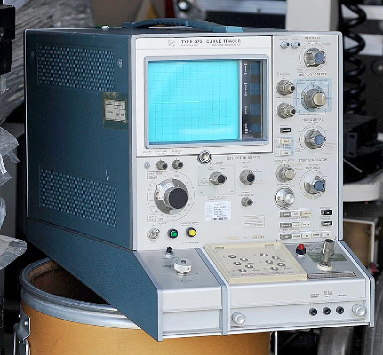
For most of the history of power semiconductor characterization, the workhorse instrument sat quietly in the corner of the lab: the curve tracer. Tektronix introduced the first commercial curve tracer in 1955, and the legendary Type 576, introduced in 1969 and capable of sweeping 1500 volts and 20 amperes through a device under, defined how a generation of power engineers understood transistors, diodes, thyristors, and IGBTs. The 576 and its successors, the 370A/B series, remained in production into the mid-1980s and are still in active use today for failure analysis and teaching.
Curve tracers are fundamentally steady-state instruments. They sweep a voltage, measure the resulting current, and plot the I-V characteristic on a screen. For silicon MOSFETs and IGBTs switching at tens of kilohertz in yesterday’s power electronics, that was enough.
That era ended with the commercial emergence of silicon carbide (SiC) and gallium nitride (GaN) power devices. Wide bandgap (WBG) semiconductors switch at rates that turn switching loss into the dominant loss mechanism. The parameters that determine system efficiency — turn-on energy (Eon), turn-off energy (Eoff), reverse recovery energy (Err), voltage overshoot, dv/dt, di/dt — live entirely in the dynamic behavior of the device during nanosecond transitions. A curve tracer cannot see them.
The industry’s answer is the Double Pulse Test (DPT), codified in JEDEC JEP182 and the IEC 60747-8/-9 standards. DPT is now a required step in datasheet generation, converter design validation, and production-line characterization at every serious power semiconductor manufacturer.
This application note covers the fundamentals of DPT briefly, then focuses on the element most often glossed over in DPT discussions: the DC bus supply that anchors every setup, and the specific engineering decisions that go into selecting one correctly.
What DPT Measures
A double pulse test extracts the dynamic switching parameters that datasheets rely on and converter designs depend on:
- Turn-on: turn-on delay (td,on), rise time (tr), turn-on energy (Eon), dv/dt, di/dt
- Turn-off: turn-off delay (td,off), fall time (tf), turn-off energy (Eoff), dv/dt, di/dt
- Reverse recovery (of the freewheeling device): reverse recovery time (trr), peak reverse recovery current (Irr), reverse recovery charge (Qrr), reverse recovery energy (Err)
These parameters feed directly into converter efficiency calculations, thermal modeling, EMI prediction, and gate drive optimization, which is why every WBG device datasheet publishes them, and why every converter designer wants to verify them on the specific parts they’re buying.
How Double Pulse Testing Works
The canonical DPT circuit is a half-bridge with an inductive load. The device under test is typically the low-side switch. The high-side device, often another MOSFET with its body diode, or a dedicated freewheeling diode, provides the current path during the freewheeling interval. A large DC-link capacitor bank supplies the pulsed energy, and a DC power supply charges the bank to the test voltage.
The three phases
A double pulse test, despite its name, has three distinct intervals.
Phase 1: Charging pulse (τc)
The DUT turns on. Current ramps up linearly in the load inductor according to:

三个阶段
双脉冲测试虽名为"双脉冲",但实际包含三个不同的时间间隔。
阶段1:充电脉冲(τc)
DUT导通。负载电感中的电流按以下公式线性上升:
第一个脉冲宽度τc的选取应使电流达到目标测试电流Itest:
At the end of this interval, the DUT turns off. This is where the first turn-off event is captured — at the target test current, with the DC bus fully charged. This is the Eoff measurement.
Phase 2: Pulse break (τoff)
The DUT is off. Inductor current circulates through the high-side freewheeling device. This interval must be long enough for switching transients to fully decay, but short enough that inductor current doesn’t drop significantly.
Phase 3 Second pulse (τon)
The DUT turns on again. Now the turn-on event is captured at the target current, with realistic di/dt conditions. Simultaneously, the freewheeling device undergoes reverse recovery, which is captured as the peak Irr spike. This is where Eon and Err are measured.

开关损耗与电容器组选型
开关损耗通过对开关过渡期间瞬时电压与电流乘积进行积分来计算。对于导通过程:
Eoff and Err follow the same form over their respective intervals. Integration limits are defined by JEDEC JEP182, typically at 10% voltage and current crossing thresholds. Modern oscilloscopes with DPT application software automate the calculation.
The DC-link capacitor bank must be large enough that the bus voltage stays substantially constant during the pulse. From energy balance, with small allowable droop ΔVDC:
实际的DPT测试装置使用数十到数千微法的并联薄膜电容,排列方式旨在最小化等效串联电感。该电容器组的容量计算公式也是电源选择计算的输入参数。
商业格局:构建DPT测试平台的三种方法
行业已形成三大类DPT测试装置。
交钥匙系统
供应商提供的全集成套件,包括栅极驱动器、测试夹具、测量设备、分析软件,有时还包括直流母线电源。例如:Keysight PD1500A、Rohde & Schwarz + PE-Systems搭配R&S MXO示波器。可快速获得测试结果,开箱即符合JEDEC标准,但电压和电流范围固定,且资金成本较高。
仪器套件
高带宽示波器加任意函数发生器、专用探头和DPT软件选件。典型代表是Tektronix 4/5/6 Series B MSO搭配WBG-DPT应用和AFG31000;Teledyne LeCroy搭配光隔离探头是另一种方案。成本低于交钥匙系统,且仪器可用于其他工作,但测试夹具、栅极驱动器、电容器组、负载电感和直流电源均需用户自行配置。
定制/自建测试平台
在半导体制造商、研究实验室以及在器件电压和电流方面追求极限的OEM厂商中占主导地位。每个组件都根据目标测试范围单独选择。对于1700 V以上的器件、大电流模块(数百安培至千安培级别)以及测试条件尚未标准化的新型器件结构,这是唯一可行的方案。
The constant across all three architectures is the DC bus supply. Every system treats it as a given. The rest of this application note covers what it actually takes to specify one correctly.
Power Supply Selection for DPT
The DC power supply in a DPT bench performs a specific and often misunderstood role. It does not source the pulsed current into the DUT directly, that energy comes from the DC-link capacitor bank. The supply’s job is to charge the capacitor bank to the test voltage and recharge it between shots, while doing so accurately, repeatably, safely, and under automated control.
That role carries specific requirements.
Voltage rating
The supply must deliver the DC bus voltage at which characterization is performed. Good practice tests WBG devices at 50–80% of their rated VDS. Practical implications:
| Device rating | Typical DPT bus voltage | Supply rating |
|---|---|---|
| 650 V GaN e-HEMT | 400 V | 500 V minimum |
| 1200 V SiC MOSFET | 800–1000 V | 1000–1500 V |
| 1700 V SiC MOSFET | 1200–1400 V | 1500–2000 V |
| 3300 V SiC module | 2500–2800 V | 3000 V+ |
| 6500 V SiC / high-V devices | 5000+ V | 6000–10000 V |
The trend line is unambiguous: device voltages are climbing. A DPT bench built around a 1500 V supply in 2020 cannot characterize the 3300 V devices entering volume production now.
Current capability and how to size it
This is where DC supply selection is most often misunderstood. The peak pulsed current flowing into the DUT during the test is sourced by the capacitor bank, not the supply. The supply’s job is to replenish the energy drawn from the capacitor bank between shots, equating to a much smaller current requirement for the supply than the peak pulse current.
There are two constraints to evaluate. The binding requirement is whichever is larger.
Energy balance (usually dominant). Each DPT shot transfers energy from the capacitor bank into the load inductor:
如果以频率fshot重复进行脉冲测试,电源必须提供的平均功率为:
最小电源电流为平均功率除以母线电压:
充电时间约束(在高脉冲频率下为约束条件)。每次脉冲测试期间,电容器组损失电荷ΔQ = CB · ΔVDC。电源必须在可用的充电时间窗口Trecharge内补充该电荷,该时间窗口通常为脉冲间隔减去脉冲持续时间和测量稳定时间:
For most laboratory characterization work, the energy-balance equation governs. For high-throughput production parametric testing, where shots are spaced milliseconds apart and capacitor banks are sized large for high test currents, the recharge constraint dominates. Calculate both and size the supply for the larger.
Example 1: 1200 V SiC MOSFET lab characterization
A typical research lab DPT setup:
Example 2: Production-line parametric testing
在此情况下,充电约束比能量平衡高出两个数量级以上,因此需要一台额定至少为 3 A、1000 V(3 kW)的电源。
实际要点
对于绝大多数双脉冲测试应用,电源的平均电流额定值比被测器件(DUT)的峰值脉冲电流低一到三个数量级。按 DUT 峰值电流来选择电源是一种代价高昂的过度规格设计,既浪费机架空间又增加预算,却毫无益处。使用上述两个公式正确选型电源后,通常会发现一台更小巧、更紧凑的电源完全能够胜任。
这正是 Magna-Power 应用工程团队直接参与的领域。我们曾为各种双脉冲测试平台选配直流电源,从大学科研实验室的单次脉冲测试台到高通量生产参数测试单元,我们非常乐意为任何特定配置详细讲解计算过程。
双脉冲测试对电源的关键特性要求
除了基本的电压和电流额定值之外,双脉冲测试平台对电源的控制、保护和物理尺寸提出了特定要求。以下各节介绍了双脉冲测试装置对其直流母线电源的具体要求,以及 Magna-Power SLx 系列和 XR 系列的相应功能——从大学研究实验室到半导体生产车间,这两个系列长期以来一直是双脉冲测试的核心设备。
编程、测量与自动化
开关损耗随 VDC、Itest、Tj 和栅极驱动条件而变化,因此在宽禁带(WBG)器件表征中,跨多个母线电压的参数扫描是常规操作。电源不仅仅是静态供电设备,它更是测量链中的一台仪器,必须能够精确编程、准确测量、在时序控制器下快速响应,并与实验室运行的各种自动化基础设施集成。
母线电压设定值最终决定了双脉冲测试测量在器件 V-I 特性曲线上的位置,而电源的电压回读值直接用于开关损耗计算。SLx 系列的编程精度低至满量程的 ± 0.06%,测量精度足够高,使得电源引入的不确定度不会在典型宽禁带器件的测量误差预算中占主导地位。
Parametric DPT characterization typically sweeps across multiple bus voltages per device, for example 400 V, 600 V, 800 V, 1000 V for a 1200 V SiC MOSFET, with DPT shots repeated at each setpoint. The supply has to move between setpoints cleanly and quickly. MagnaLINK distributed DSP digital control on the SLx Series implements programmable slew rates and fast programmable ramping with field-tunable gains across a wide range of load conditions, letting an automated sweep sequencer step through a full voltage-current-temperature matrix.
Digital commands over a network interface has inherent latency typically milliseconds, which can introduce jitter into tightly-coordinated DPT sequences. For applications where the supply's state needs to synchronize with the gate driver, AFG, and oscilloscope without going through the command layer, the SLx and Series provides a standard D-Sub User I/O with analog and digital logic. This I/O provides a hardware path for real-time feedback and control that's independent of the software command interface, allowing the supply can be wired directly into the test bench's interlock system, trigger logic, and analog measurement paths.
Automation infrastructure varies widely across the DPT customer base, including LabVIEW, Python over Ethernet, IVI drivers in TestStand, production floors running PLC controlled sequencers. The supply needs to integrate with whichever infrastructure is already in place, not force a change in it.
The SLx Series comes standard with dual USB (front and rear) and RS-485, with full SCPI and Modbus command-set support. Optional LXI TCP/IP Ethernet (+LXI) provides standard lab network control, and for environments running industrial automation, SLx additionally offers CANopen, EtherCAT, EtherNet/IP, ModbusTCP, and PROFINET as fully-integrated communication options, each with full command-set support, enabling direct control from industrial PLCs (Siemens PROFINET being particularly common in semiconductor fabs and automotive test cells). The XR Series comes standard with serial RS-232 and supports LXI TCP/IP Ethernet (+LXI) and IEEE-488 GPIB (+GPIB) as optional interfaces for broader lab instrumentation integration. National Instruments LabVIEW and IVI drivers are included with every supply.
Starting from Python–what Magna-Power uses in-house for its own test software–is straightforward the supply listens on a socket, SCPI commands are ASCII text, and a full DPT sweep scaffolding with logging takes a dozen lines:
import socket, time

# Connect to supply at lab network address, default SCPI socket port
s = socket.socket(socket.AF_INET, socket.SOCK_STREAM)
s.connect(('192.168.0.86', 50505))

# Identify and configure for remote control
s.sendall(b'*IDN?\n')
print(s.recv(4096).decode())
s.sendall(b'CONF:SOUR 0\n')

# Sweep across bus voltages for parametric DPT characterization
for v_bus in [400, 600, 800, 1000]:
    s.sendall(f'VOLT {v_bus}\n'.encode())
    s.sendall(b'OUTP:START\n')
    time.sleep(0.1)   # settle time before DPT shot
    # [trigger AFG, capture scope waveforms, calculate E_on/E_off]
    s.sendall(b'MEAS:ALL?\n')
    curr, volt, pwr = s.recv(4096).decode().split(',')
    print(f'V_bus={v_bus}: measured {float(volt):.2f} V, {float(curr):.3f} A')

s.sendall(b'OUTP:STOP\n')
s.close()
Self-protecting topology under load faults
DPT is inherently destructive testing. Devices routinely fail, and when they do, they typically short. The supply must respond to a load fault without cascading into supply damage, without injecting large reverse currents back into the capacitor bank, and without releasing stored energy in ways that propagate damage through the bench.
Every MagnaDC power supply supply is built on Magna-Power's signature current-fed power processing topology, which adds a control stage over conventional voltage-fed designs. Under fault conditions, this topology inherently limits fault energy: no fast-rising current spikes, no magnetic core saturation, and self-protecting behavior under short-circuit loads. For DPT applications, this is the first line of defense when a DUT fails: the power supply architecture itself resists the fault, rather than relying on firmware-controlled trip responses. Combined with the safety protections in the following section, the SLx Series and XR Series tolerate repeated DUT-failure events without taking the bench down.
Safety protections
DPT pushes devices to failure by design. A well-designed supply provides multiple layers of protection that together shield the supply, the bench, and the operator from the range of things that can go wrong, DUT shorts, runaway currents, overvoltage transients from the cap bank, thermal excursions, enclosure breaches, and operator errors. The protection strategy is layered rather than single-point: each mechanism operates independently, so no single failure defeats the whole system.
Programmable overvoltage trip (OVT) and overcurrent trip (OCT) are the first programmable layer. Both SLx Series and XR Series supplies provide OVT and OCT settings configurable from the front panel, User I/O, or via command interface, with trip thresholds independent of the output regulation setpoint. For DPT, OCT is typically set a modest margin above the expected recharge current so that any anomalous load behavior.
For thermal protection, distributed thermal switches monitor multiple points inside the supply, and control-integrity diagnostics watch the programming line, remote sense leads, and internal references. A fault on any of these conditions trips the supply independently of the programmable OVT/OCT settings.
A dedicated Interlock hardware input that inhibits the output when a contact loop is broken with a latching fault. The Interlock typically integrated with the test enclosure: a 5V-referenced dry-contact loop runs through the enclosure door, the fixture cover, and any other safety-critical interlocks. Opening any link disables the output. Both the SLx Series and the XR Series provide an interlock input as a standard feature; this is the baseline hardware safety layer that every DPT bench should tie into its enclosure and access controls.
A dedicated hardware emergency stop is available on the SLx Series as an additional layer. The E-stop input, when triggered by a 24V signal, creates an AC-interrupt path that bypasses all logic, processors, and control firmware. This provides a hardware-only shutdown mechanism independent of the supply's control electronics, which is useful in installations where an additional layer of hardware isolation beyond the interlock is desired.
Combined, these mechanisms let the supply tolerate repeated DUT failures — the kind of destructive testing that characterization work actually requires, without propagating damage through the bench.
Rack Density
DPT setups are instrument-heavy: oscilloscope, function generator, gate driver supply, thermal chamber controller, automation hardware, and the DC bus supply.
Magna-Power's SLx Series delivers up to 10 kW at voltages to 3,000 Vdc in a single 1U chassis, where a conventional high-voltage programmable supply typically occupies 3U or more. Part of the reason is architectural: many competitive supplies include auto-ranging output stages to offer constant power across a wide envelope, which adds parts count, cost, control complexity, and physical volume. For DPT, the test voltage is set by the DUT and the average current demand is known from the sizing analysis; auto-ranging. Fixed-range supplies sized for the target device class deliver the same useful capability in less space at lower cost.
Where DPT Is Going
Several trends in wide bandgap device development are directly relevant to the DC supply side of the DPT bench:
- Higher voltages. 3.3 kV SiC is in volume production. 6.5 kV and 10 kV SiC devices are moving from prototype to early commercial availability. DPT bus voltage requirements are climbing with them.
- Higher currents and module-level testing. Characterization at hundreds of amperes to kiloamperes is increasingly common, which raises energy-per-shot and capacitor bank recharge rate — exactly the parameters that make Section 5.2’s recharge constraint dominate over energy balance.
- Tighter integration with reliability testing. DPT is no longer standalone; it’s integrated with HTRB, HTGB, and power cycling on the same bench, which makes supply stability over long test durations a more demanding requirement.
- Automation at the production line. Parametric DPT on every production unit is becoming routine for some manufacturers, shifting the bottleneck from measurement to capacitor bank recharge time.
In every one of these directions, the DC bus supply requirements climb. The SLx Series at 3 kV and the XR Series at 10 kV are positioned to follow the devices upward, in the 1U and 2U form factors that keep the rest of the DPT bench buildable.
References
Wang, F., Zhang, Z., and Jones, E. A. (2018). Characterization of Wide Bandgap Power Semiconductor Devices. IET Energy Engineering Series, Vol. 128. Stevenage, UK: Institution of Engineering and Technology. ISBN: 978-1-78561-491-0.
IEC 60747-9:2019, Semiconductor devices – Discrete devices – Part 9: Insulated-gate bipolar transistors (IGBTs), Edition 3.0. Geneva: International Electrotechnical Commission, November 2019.
JEDEC Solid State Technology Association (2021). JEP182: Test Method for Continuous-Switching Evaluation of Gallium Nitride Power Conversion Devices, Version 1.0. Arlington, VA: JEDEC.