Learn White Papers
Power Electronics Hardware Design for Manufacturability
This article was written by Magna-Power Electronics and originally appeared as the cover story in the Q4 2021 issue of the IEEE Power Electronics Magazine. DOI: 10.1109/MPEL.2021.3123832
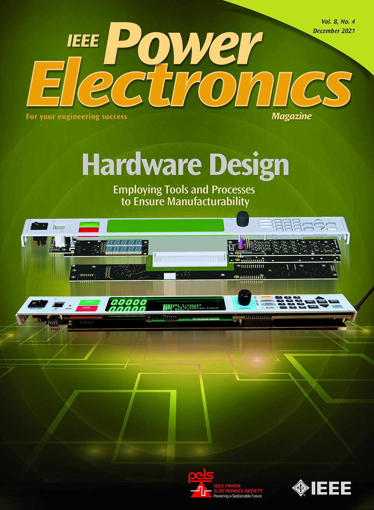
With a small, diverse team of engineers, Magna-Power Electronics can offer over 250,000 different configurations of programmable power supplies and electronic loads, spanning current levels up to 10,000 Adc, voltage levels up to 10,000 Vdc, and power levels up to 3,000 kW. This feat is made possible through tightly integrated engineering and manufacturing teams, minimizing labor and maximizing automation, and imposing consistency as a core principle across all designs. This article shares several strategies within the power electronics design process that the company has iterated on during its 40-year history, including printed circuit board (PCB) design and vendor selection, prototype and design controls, and electro-mechanical integration. While Magna-Power has nearly fully in-sourced manufacturing operations under one roof, the strategies presented can also be implemented through close vendor relationships and understanding of the constraints from various production processes and machinery.
Printed Circuit Board Design
PCB fabrication is one of the few manufacturing components that the company outsources. It is also the most complicated component to specify, revise, and manage inventory. Correctly communicating design requirements to the PCB manufacturer, along with observing their individual fabrication constraints, allows designs to be fungible across manufacturers; such a process has been refined over many years through experimenting with many different vendors. Supporting multiple product lines requires maintaining a pool of manufacturers with different specialties. Some excel at fine pitch and multiple layers, others specialize in high-ounce copper and/or high-temperature tolerant fiberglass, and some for quick-turn around prototypes that operate 24 hours/day, 7 days a week. Multiple manufacturers from different regions have added much resilience to our supply chain, which is advantageous when a country shuts down for holiday, and recently due to COVID-19.
The next two sections explore manufacturing considerations for high-voltage and high-current layout design and fabrication. Each consideration is presented followed by images of real-world consequences when ignored.
High-Current Printed Circuit Boards
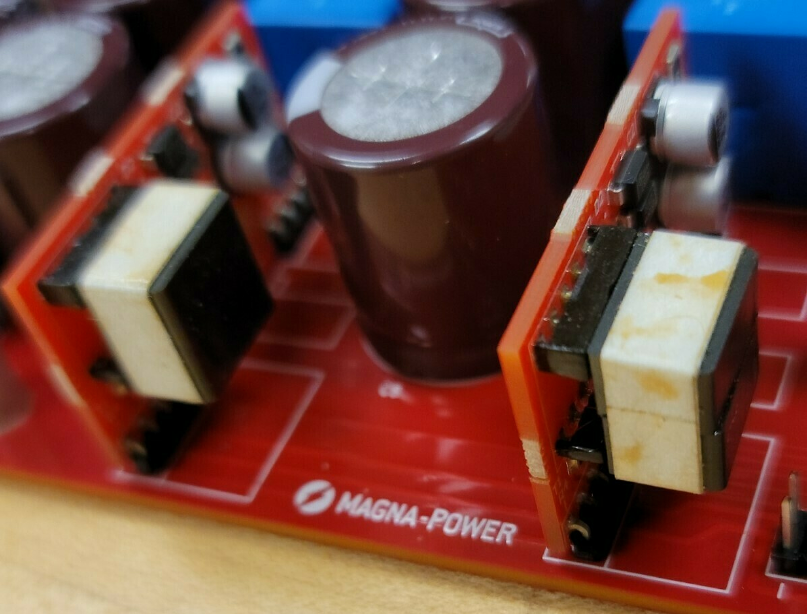
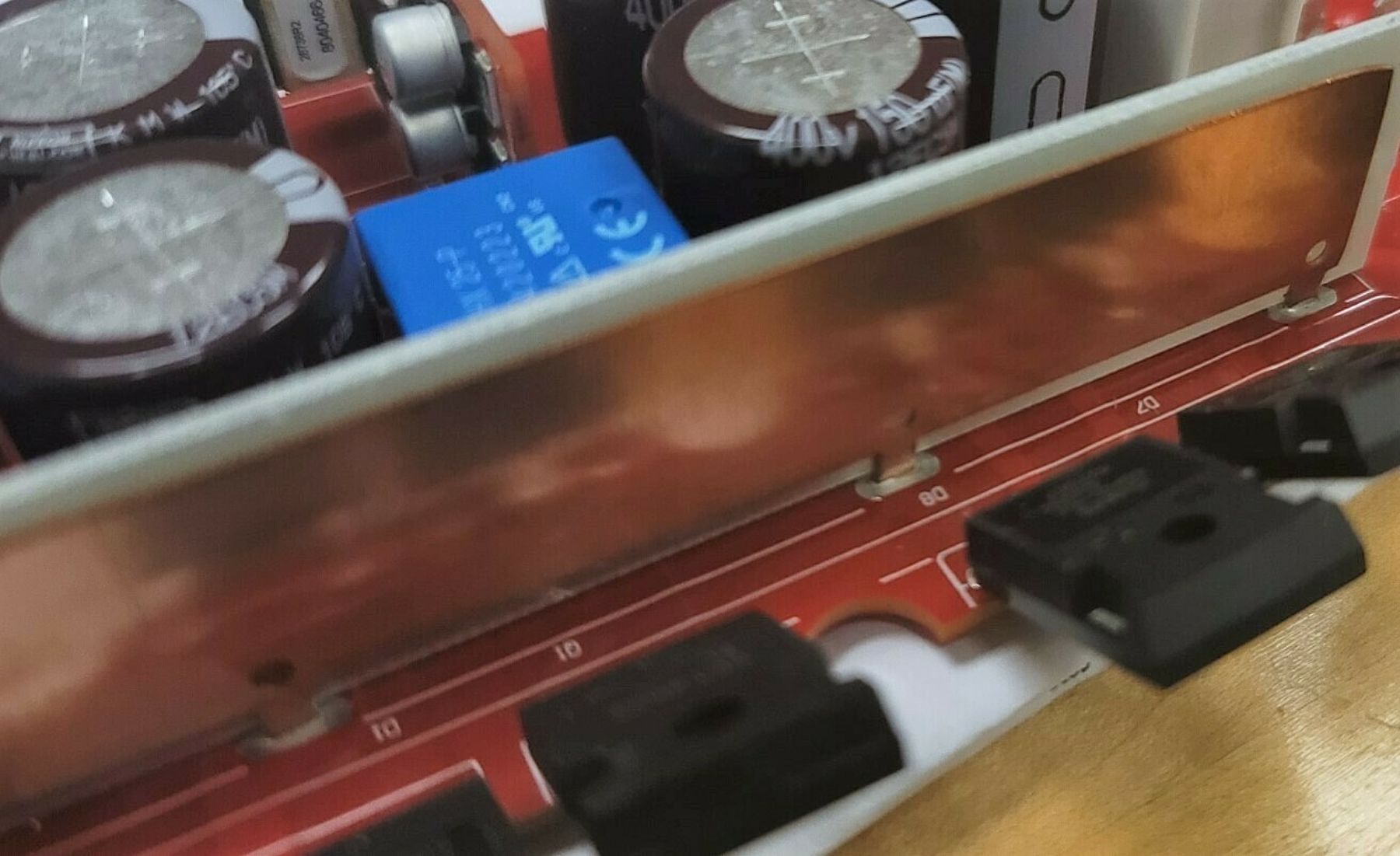
The current a PCB can handle is governed by the thickness of copper, specified in ounces, and the number of conductors, specified in layers. Working with thick copper (high ounce) clad FR4 introduces challenges both on the board fabrication side as well as the circuit assembly, mostly rooted in chemical and machinery limitations. Thick copper (which for Magna-Power is 4 oz or more) is more difficult to acid etch, and the PCB fabricator will have wider tolerances and alternative design guidance. For example, one of our board manufacturers recommends 5 mils minimum trace width for 1 oz copper. This recommendation jumps to 15 mils for 4 oz copper. Wider trace limits the selection of digital ICs than can be installed on a board. Mobile computing has been driving chips smaller, shrinking the pitch on IC packages, whose leads are often too tightly spaced for trace routing on power boards. The workaround for this problem is to consolidate logic and control circuitry to a light-ounce PCB that mates with high-ounce PCBs, as shown in Fig. 1.
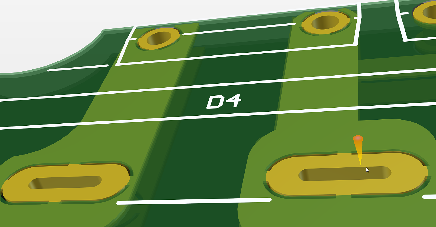
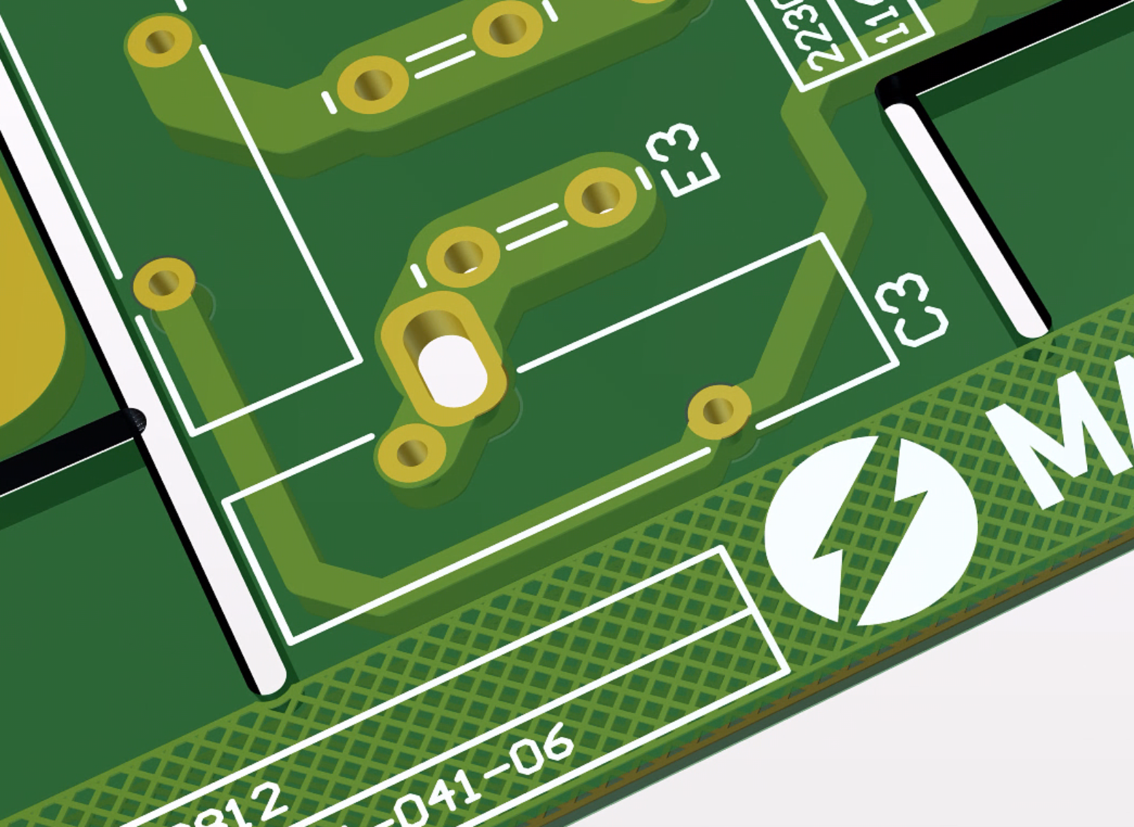
Copper is an excellent electrical and thermal conductor. The latter is undesirable for manufacturing as it sinks heat away from joints, lowering the temperature below what is necessary to melt solder completely. Thermal reliefs, as shown in Fig. 2, are recommended for any copper pour to pad connection so that production can solder more easily. Single high-current PCB pads (terminals, bus tabs, etc.) should be split into multiple parallel connections. Doing so produces the same current output while increasing the thermal conductance of each joint, which eases soldering, as shown in Fig. 3. Since most through-hole assemblies pass through a wave solder machine, where joints are soldered all at once, the added connections have no impact on labor and makes any solder iron rework more efficient.
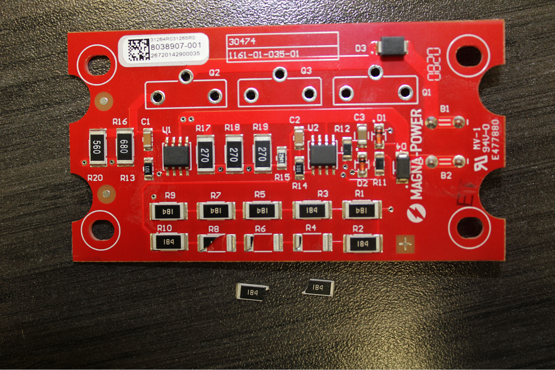
Most Magna-Power PCBs retain a thickness of 62 mils, which is the common layer stack-up in industry. For high-current PCBs, each copper layer is 5.6 mils, so when multiple layers are needed, the core thickness is increased to keep the final assembly rigid. On a 4 oz, 4 layer PCB, Magna-Power designs use a 59 mil dielectric core and a total board stack-up of 92 mils. The core thickness will keep the board flat on the pick and place machine, leading to more accurate component placement, and prevents warping caused by heat in the wave or reflow oven. PCB flex caused by general handling, insertion of heavy components (transformers, heatsinks) can cause cracked surface mount resistors and capacitors. Placing components too close to a board edge is a common design mistake that is quickly identified in the production process; applied pressure of a de-paneling saw flexes the PCBs enough to crack delicate MLCC capacitors, and even thick-film resistors, as shown in Fig. 4.
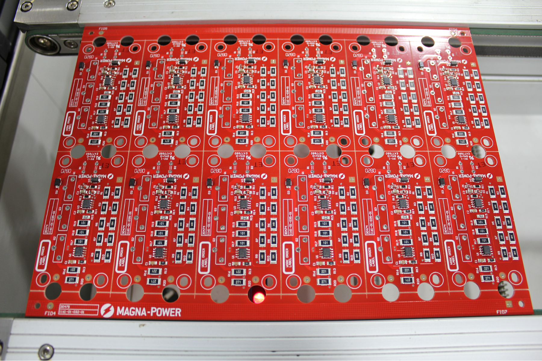
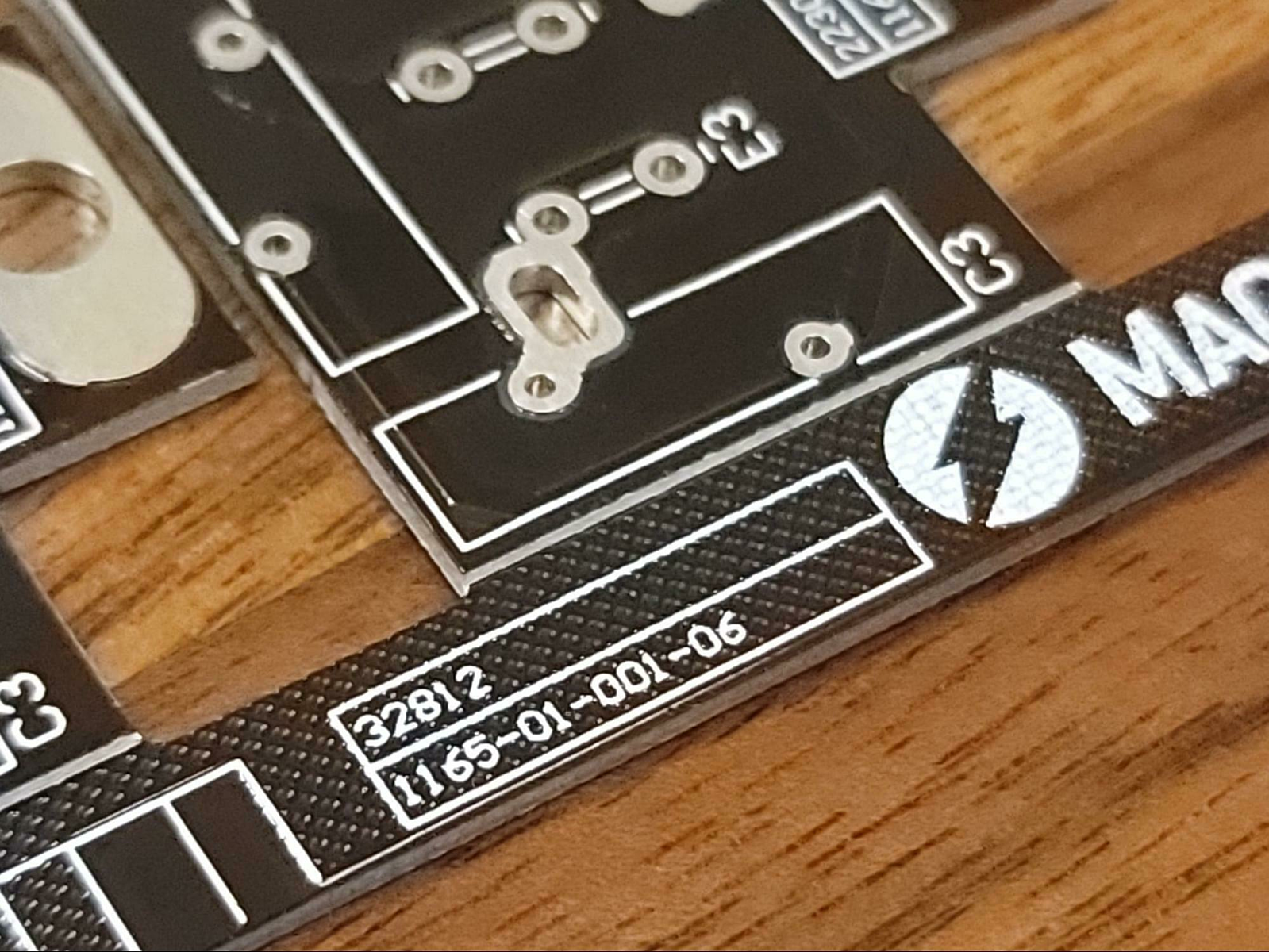
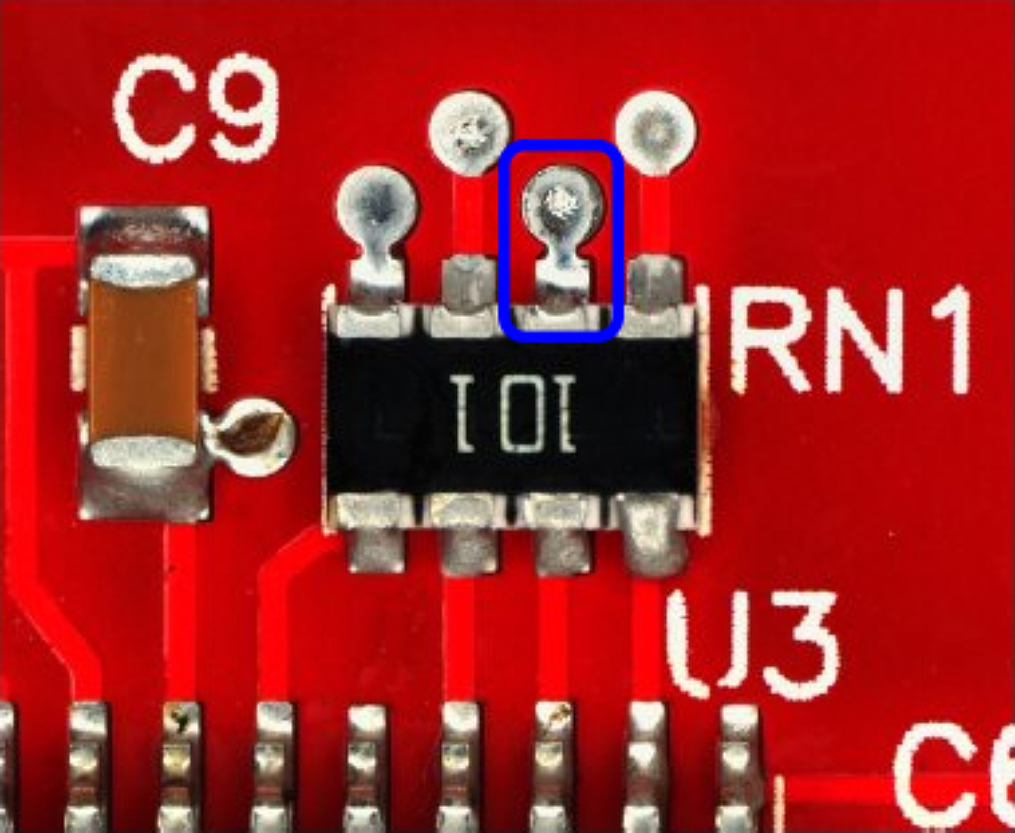
One should internalize the PCB manufacturer’s fabrication limitations, which change with copper ounce offerings. One critical, non-obvious constraint is the minimum solder sliver, which describes solder mask print resolution. For example, one PCB manufacturer specifies 8.5 mils mask for 1 oz copper and 11.5 mils for 4 oz. Our long-time vendor explained that thick copper raises the surface more, which causes issues in the masking process, which expects a flat surface. Multiple passes across the solder mask screen may be needed to fully coat the top surface and fill the ridges between the copper and dielectric, which also increases the required tolerance. PCB fabricators will often remove the solder mask automatically when spacing is too small, resulting in soldering defects. Without a mask, pads on the same node bridge together as shown in Fig. 5, and vias can wick solder away from a mounted chip, starving leads of solder, resulting in solder defects [1] as shown in Fig. 6.
High-Voltage Printed Circuit Boards
There are many machinery specific constraints that must be considered in high-current PCB design. For high-voltage PCB design, these constraints are mostly electrical. Tracking constraints across copper ounces and manufacturers would be arduous and prone to human error if done manually. Design rules within PCB design software are used extensively at Magna-Power to document and automatically enforce complicated and varied constraints, on-the-fly. Discovered defects in a PCB design are permanently stored, versioned, and enforced in either a design rule for the project, universally through a design rule library, or using a master library footprint. By storing defects this way, a discovery is shared among the entire engineering team, and not repeated in future projects. The two major design rules for high-voltage PCB design are clearance and creepage. Nets with high and low potential are identified and grouped, and distance rules between them are set based on the worst-case voltage and recommendations in IPC-2221 [2]. The advantage of rule-based design is that copper pours will automatically adjust to satisfy the design rules while providing maximum allowed copper in each area. A constraint routed ceramic capacitor on our high-voltage output assembly is shown in Fig. 7. In this example, the creepage has a higher priority than clearance, so the design rule checker will approve the design despite failing the clearance. In addition, note how the clearance rule precisely chisels out copper in high-potential areas.
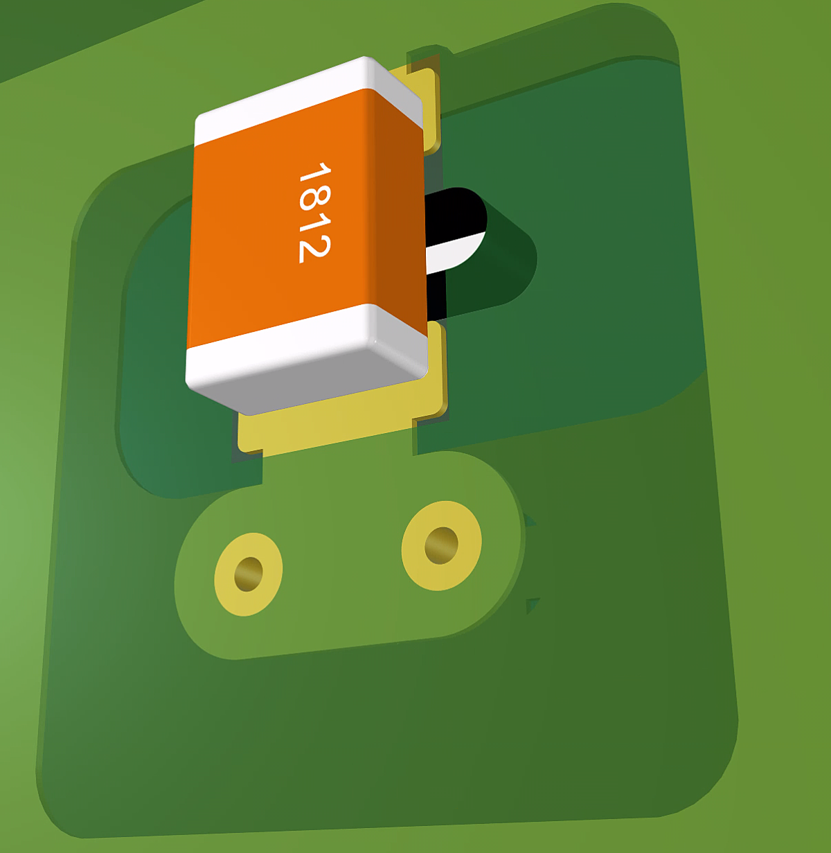
The creepage distances selected also depends on the production process implemented. IEC 60947-1 [3] shows that surface pollutants and dielectric material reduce creepage, which for power supplies, translates to lower power density. Milling slots into dielectric, as was done in Fig. 7, has been shown experimental in [4], to increase the breakdown voltage by 20%. All Magna-Power products are standardized, precision, rackmount equipment, operated in reasonably clean laboratory (pollution degree 2), and designed accordingly. Spacing for the input stages are designed for 1.2 kV worst-case (480 V at 3ф line source). Output stage spacing is defined by the dc output voltage rating. At the extereme, is Magna-Power’s XR Series power supplies (ranges up to 10 kVdc output), the PCBs on the output section are all washed after production to prevent arcs. Most other low-voltage assemblies use a no-clean process, which is less labor, at the cost of residual flux (pollutants). High-voltage assemblies also should avoid sharp edges, which can become arc points. Edges can be avoided by enforcing acute angle design rules in software, routing with rounded traces and pours, and flush cutting leads on through-hole components, as shown in Fig 8. Despite all these design rules and production precautions, debris can still unintentionally contaminate high-voltage areas (e.g., metal shavings from inadequate deburring). Therefore, all products 1 kV and greater are hipotted before any factory testing begins.

Managing Prototypes for Internal Manufacturing
Effectively tracking and managing prototypes alongside production work orders has been a long-term challenge at Magna-Power, requiring many iterations in business logic and record keeping. The objective is to treat a prototype job like any standard job, and have it follow standard production procedures. Exposing new designs to as many processes as possible will reveal electrical as well as manufacturing defects and is a key advantage to insourcing. Setting up a small production/prototype run requires some up-front record keeping: all components must be entered in the database, the Bill of Materials (BOM) completed, purchase orders signed, Work Orders (WO) issued, and jobs kitted. Catching record keeping errors, while not glamorous, is an equally important task. Waiting until mass production to find these errors can become a very expensive mistake. This section describes Magna-Power’s approach to record keeping and versioning needed for manufacturing to read a design, as well as the custom software tools developed to support record entry and validation, and finally the engineering retrospectives in post-production–all which keeps costly design iterations to a minimum.
Document Control
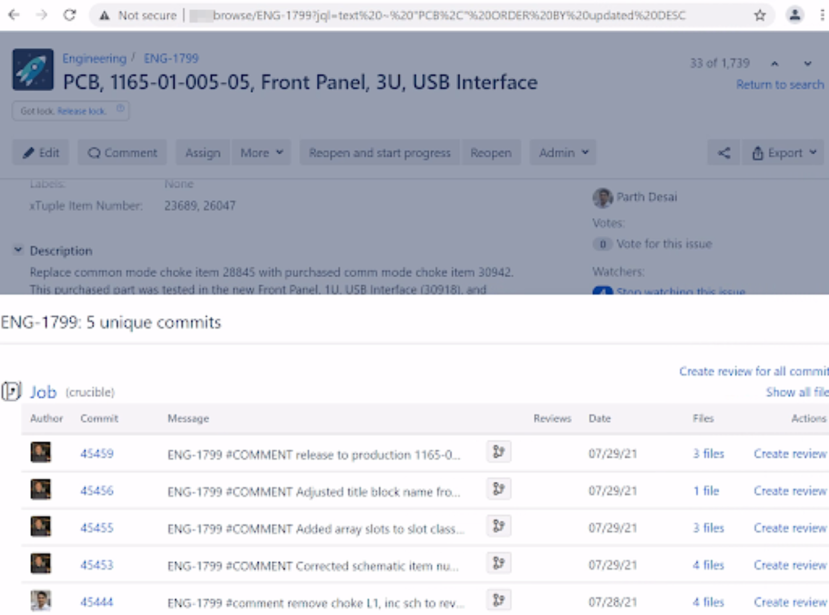
Most production departments rely on engineering drawings to bring designs into reality. New drawings and modifications originate from a feature, issue, or improvement in a product; reported by production, management, sales/marketing, or a customer in the form of a ticket. The engineer assigned this ticket will research and group related tickets together such that multiple tickets can be resolved/advanced in the same prototype run. When drawings are first created or modified, they are committed to a working folder in a file version control system. Each change is linked back to the original ticket, providing a complete historical record of file changes along with justifications, all in one location, as shown in Fig. 9. In a version control system, no file is ever deleted, only those authorized can view or modify files, everyone has centralized access, and two engineers are blocked from overwriting another’s work. Such a system is needed when working in a highly collaborative engineering/manufacturing environment. The same version control is used for schematics, layouts, mechanical drawings, magnetics drawings, and source code. This system is even used for storing complicated pick and place recipes and robotic machine programs, so that jobs can be recalled quickly and are repeatable. The company’s implemented ticket/version control system solved a major cultural conflict between the worlds of engineering and production. Engineers thrive on change and improvement, while manufacturers thrive on quality and repeatability. The ticket provides the reasoning to production to justify change, while versioning locks in a design and ensures repeatability.
Production Records
Engineers responsible for the initial document design are also the ones that first create new records for components and BOMs. Companies’ that clearly separate engineering, manufacturing, and planning will often end up with duplicated record keeping systems that are unsynchronized and prone to error. Magna-Power’s vertical integration along with its centralized records affords data sharing among design tools and manufacturing equipment, the advantages of which are discussed in this section.
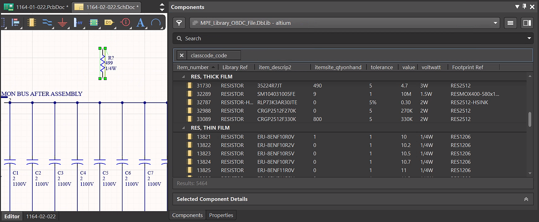
The most important record strategy an engineer can take when entering new components is to avoid entering new components as much as possible. The engineer should use existing components in the supply chain and introduce new components only when it is a necessity. Is that 1% resistor really needed, or will an existing 5% resistor from the stockroom suffice? Much effort goes into vetting vendors, validating authorized distributors, negotiating pricing, setting reorder levels, and inventory control records. On the manufacturing side, pick and place machines have limited feeder lanes. Part consolidation reduces the reel changeover, which reduces labor, and less handling lowers chances for picking errors. To encourage material reuse in new designs, Magna-Power integrated its central database into its schematic and layout software. In the schematic design, only the active components are shown, along with live inventory levels, as shown in Fig. 10. Dragging the part into the schematic adds the footprint, symbol, and around ten associated properties–its simplicity encourages existing components reuse. Custom software was programmed to take a schematic and inject it back into the database. For complicated boards, like the company’s new generation digital control board, which contains over 400 components, the BOM was injected into the enterprise resource planning software in one button click.
As a design matures, engineering may make tweaks to fix problems or implement features, or planning may replace components as they become obsolete or hard to acquire. In these situations, human error will inevitably occur; engineering may forget to update a BOM or planning may fail to tell engineering to revise a schematic. Such errors result in design documents becoming out of sync with BOMs and production confused which is correct. To safeguard against this problem, custom software was created that runs when the PCB department creates recipes for the pick and place machine. The software compares the BOM against the schematic/layout and logs discrepancies. The software cross references designators (e.g. R1, C43, etc.), part numbers, component properties (values, voltage, wattage, tolerances), as the final sanity check before going to production. Component property referencing is most vital, since the pick and place machine compares loaded properties cross-referenced with physical measured resistance and capacitances to verify the correct reel was installed into the feeder location before placement.
Record versioning happens at a couple key points after release to manufacturing (RTM). Magna-Power will lock in a revision for a document (tag) after the first article of inspection (FAI), when no additional changes are possible. For example, a PCB layout is tagged after it comes back from the board house, since engineers will often make corrections for the fabricator after releasing the artwork. A similar philosophy is applied to activating BOMs. When the completed assembly finishes testing, the design engineer performs a retrospective. This engineer will review feedback on all the production tickets, so they can make an informed decision. If the prototype run went poorly, the engineer may choose to just deactivate the pending revision, keep the existing, and try again on a new pending revision. Care and consideration is needed since activating a BOM or PCB clears planning for mass production and large-volume material purchasing.
The ticketing system provides a clear documentation trail as it passes through multiple processes and departments. The retrospective provides time before resolving a ticket for the engineer to review and validate the problem was indeed resolved, identify areas for improvement, and spawn new tickets for the next design cycle. The workflow’s success depends heavily on departments’ diligence on reporting issues through tickets and engineers being actively engaged in the production process.
Firmware and Software Version Controls
Magna-Power’s workflows, versioning, and tools described for hardware were adopted from those more commonly found in software development. Software developers have long since addressed the problem of managing multiple digital files among multiple people. These developers also learned to break large programs into smaller components, build, validate, and tag/version the stable revisions. These practices, when used on an entire electronic product, takes on even higher levels of sophistication.
Magna-Power’s latest digital platform has separate codebases for firmware and bootloaders (consisting of five different processors and ten code projects), programs for computer control, automated test, LabVIEW drivers, and even documentation. The source of complexity is that software projects have dependencies with each other and with hardware. Both software and hardware undergo continuous improvements to address customer needs. Examples of complexities arising from this continuous improvement include:
- a specific revision PCB needed for the latest revision BOM;
- new firmware features that may only be available for a range of BOM revisions;
- processors that can only talk to each other if they are on the same firmware version;
- a computer that can only talk to firmware if they are using the same communication protocol version;
- persistent memory in EEPROM that must adapt to firmware changes as saved settings for features are added, modified, and removed.
Magna-Power chose to address these complexities through a sophisticated, custom developed continuous integration server (CIS), designed to detect code changes then compile, test, encrypt, package, tag, and deploy software both internally and for customers. CIS hides this growing complexity from engineering and production so that staff can focus their energy on development/production and not backward/forward compatibility or tooling challenges. This CIS server, combined with state-based model design, has allowed a single firmware development to work with power supplies, electronics loads, and other special application products, while allowing customers to upgrade firmware at any time over the internet. Boards sent as replacements automatically upgrade themselves by flashing from files on the main board, and product-to-product connections (master/slave) can trigger cross-product firmware updates; to date up to thirty-seven processors formed a network and upgraded their various firmware.
Electronic and Mechanical Integration
An electronic assembly can be composed of multiple PCB assemblies, metal assemblies (standoffs and inserts), plastic parts, rubber parts, and magnetic components. The assembly’s design and construction involves multiple engineering teams and manufacturing departments. Vertical integration provides the agility for drastically shortening prototype cycles and communicating quick changes, providing visibility for catching manufacturing problems mid-cycle and improving overall quality of goods.
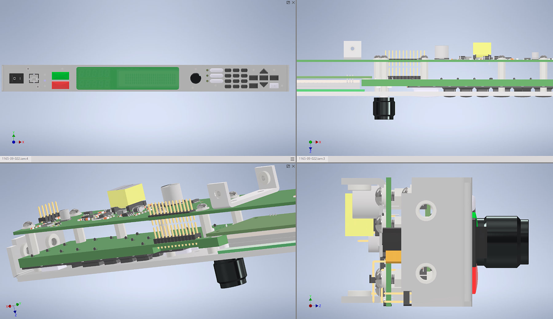
Parametric modeling has been the latest Magna-Power tool to help check the mechanical fit of electronic assemblies before physically building them. Every prototype cycle is expensive in terms of time, materials, tooling, and opportunity cost ––the motivation is high to get as much correct on each pass as possible. An example of effective parametric modeling was in Magna-Power’s new generation digital front panel, shown in Fig. 11. The design required layering multiple PCBs to fit a VFD display, keypads, light pipes, rotary encoder, ten seven-segment LEDs–all into 4.4 cm vertical height. The electronics, firmware, and metal were designed across multiple internal teams, along with some external collaborators for keypads, Lexan, and printing pads. For this design the electrical team defined 3D bodies for all components so that an accurate 3D representation could be imported into the modeling software. The mechanical team used the PCBs to determine board mounting locations, add standoffs, and create openings for the rubber keypads. The electrical team was provided a front-facing panel drawing, which was imported into the board layout software to lock in strike positions for the carbon pads. This back-and-forth process illustrates the required communication between teams and data exchange between software. For this project, most design flaws were discovered before entering production. Some flaws did make it through, such as neglecting the thickness of the power coating on the keypad openings. However, owning the punch press and power coating system allowed for quick corrections, making unanticipated flaws more manageable. The main bottleneck for the project was the only outsourced component: the keypad.
Conclusion
Design consistency is a key principle that has remained constant through Magna-Power’s history. As an engineer gains experience, this consistency becomes intuition. This agility is paramount to the company’s success, allowing it to support an extremely broad product offering with a relatively small team. While design consistency has remained constant, the strategies to achieve this principle have (and continue) to evolve as the company grows. Software-based tools were presented that enforced constraints on the design process, shared component and rule libraries, validated prototype workflows, and automated production records checks against design files. Designs must also consider processes, equipment limitations, and standards, as was described through Magna-Power’s experiences working with many PCB vendors, where the company’s own internal production processes and several key PCB design strategies were specified.
About the Authors
Grant Pitel (gpitel@magna-power.com) is the chief technology officer at Magna-Power Electronics, Flemington, NJ, USA. He obtained his M.S. and Ph.D. degrees in electrical and computer engineering from the University of Illinois Urbana-Champaign, IL, USA.
Adam Pitel (apitel@magna-power.com) is the chief executive officer at Magna-Power Electronics, Flemington, NJ, USA. He received the M.Eng degree from Princeton University, NJ, USA.
References
[1] "IPC-2221B", Generic Standard for Printed Board Design, November 2012.
[2] "IPC-A-610H", Acceptability of Electronic Assemblies, September 2020.
[3] “IEC 60947-1:2020”, Low-voltage switchgear and control gear - Part 1: General rules, April 2020.
[4] J. Maxwell and E. Lemus, “Arc Season and Board Design Observations” presented at the Capacitor and Resistor Technology Symposium, Orlando, FL, USA, 2006.
Stay connected and informed.
Subscribe to receive emails—no more than once per month—with new technical articles, product releases and factory updates from Magna-Power.
