


电力电子硬件的可制造性设计
本文由Magna-Power Electronics撰写,最初作为封面文章发表于2021年第四季度的IEEE Power Electronics Magazine。DOI: 10.1109/MPEL.2021.3123832
凭借一支小而多元化的工程师团队,Magna-Power Electronics能够提供超过250,000种不同配置的可编程电源和电子负载,电流范围可达10,000 Adc,电压范围可达10,000 Vdc,功率范围可达3,000 kW。这一成就得益于工程和制造团队的紧密整合、劳动力的最小化与自动化的最大化,以及将一致性作为所有设计的核心原则。本文分享了该公司在其40年历史中不断迭代优化的几项电力电子设计策略,包括印刷电路板(PCB)设计与供应商选择、原型与设计控制,以及机电一体化集成。虽然Magna-Power几乎将所有制造业务集中在同一屋檐下,但所介绍的策略也可以通过紧密的供应商合作关系以及对各种生产工艺和设备约束的深入理解来实施。
印刷电路板设计
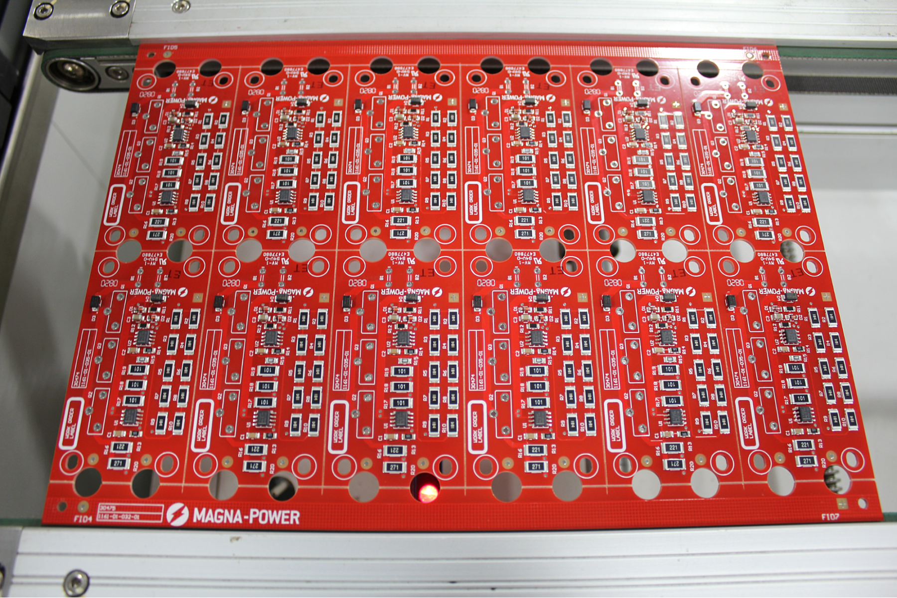
PCB制造是公司少数外包的制造环节之一,同时也是最复杂的需要规格说明、修订和库存管理的组件。正确地向PCB制造商传达设计要求,同时遵循其各自的制造约束,使设计可以在不同制造商之间灵活切换;这一流程经过多年与众多不同供应商的合作实践不断完善。支持多条产品线需要维护一个具有不同专长的制造商池。有些擅长细间距和多层板,有些专注于高盎司铜和/或耐高温玻璃纤维,还有一些则擅长全天候运营的快速周转原型制造。来自不同地区的多家制造商大大增强了我们供应链的韧性,这在某个国家因假期停工时非常有利,近期的COVID-19疫情期间更是如此。
接下来的两个部分将探讨高压和大电流布局设计与制造的注意事项。每个注意事项之后都附有忽略这些要求时实际产生后果的图片。
大电流印刷电路板
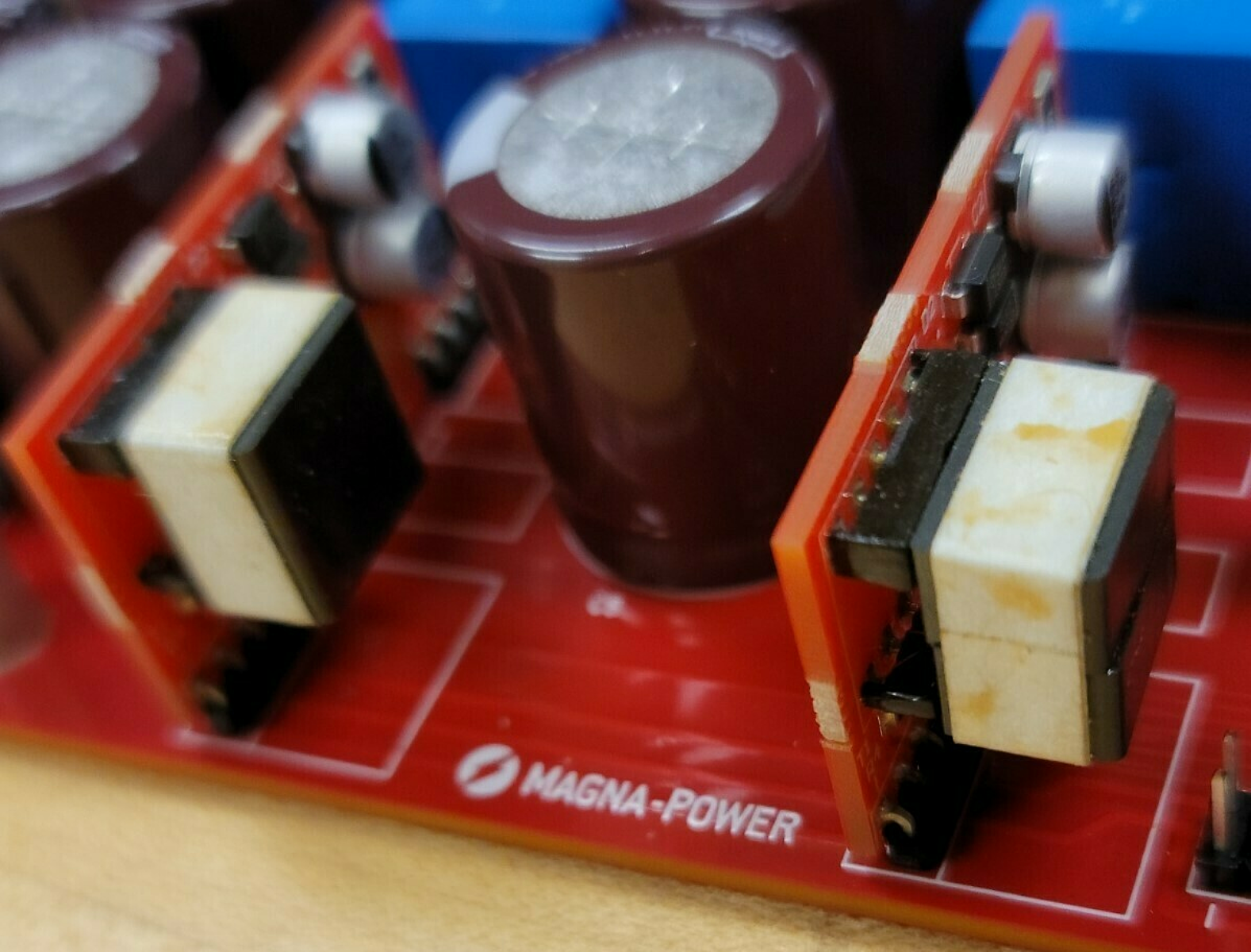
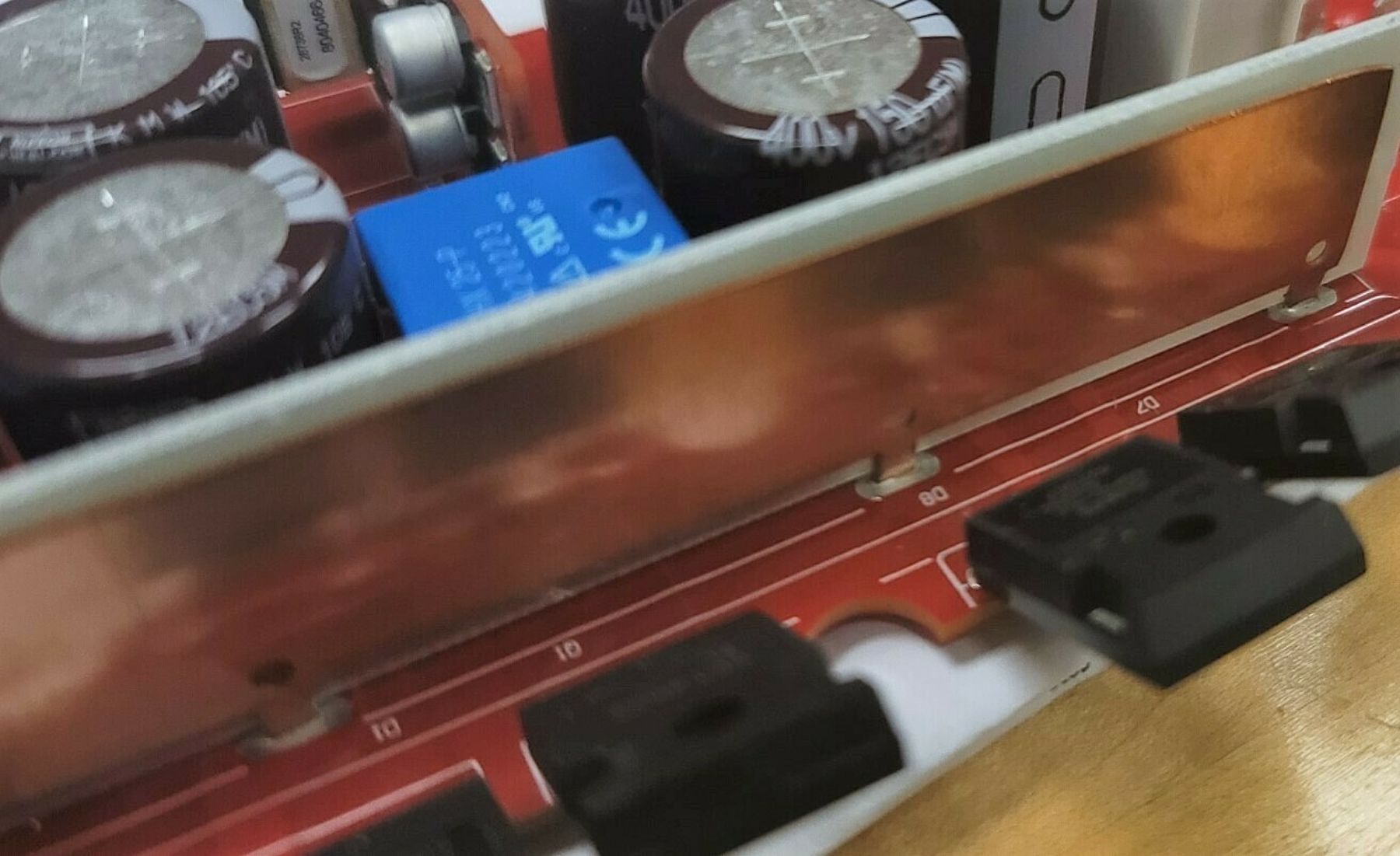
PCB的载流能力取决于铜的厚度(以盎司为单位)和导体数量(以层数为单位)。使用厚铜(高盎司)覆铜FR4在电路板制造和电路组装方面都带来了挑战,主要源于化学和设备的限制。厚铜(对于Magna-Power而言为4盎司或以上)更难进行酸蚀,PCB制造商的公差会更大,并会提供不同的设计指导。例如,我们的一家电路板制造商建议1盎司铜的最小线宽为5 mil,而4盎司铜则跃升至15 mil。更宽的线宽限制了可安装在电路板上的数字IC选择范围。移动计算推动芯片不断缩小,IC封装引脚间距也随之缩小,其引脚间距往往过于紧密,无法在功率板上进行走线。解决这一问题的方法是将逻辑和控制电路集中在低盎司PCB上,再与高盎司PCB配合使用,如图1所示。
铜是一种优良的电和热导体。后者对制造而言并不理想,因为它会将热量从焊点传导走,使温度降低到不足以完全熔化焊料的程度。如图2所示,建议在任何铜箔覆盖区域与焊盘的连接处使用热隔离(thermal relief),以便于生产焊接。单个大电流PCB焊盘(端子、母线片等)应拆分为多个并联连接。这样做在产生相同电流输出的同时,提高了每个焊点的热导率,使焊接更加容易,如图3所示。由于大多数通孔组装都会经过波峰焊机一次性焊接所有焊点,增加的连接不会影响人工成本,并且使任何烙铁返修工作更加高效。
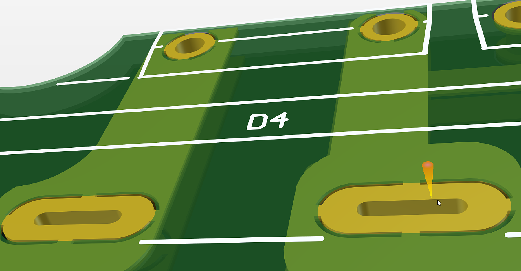
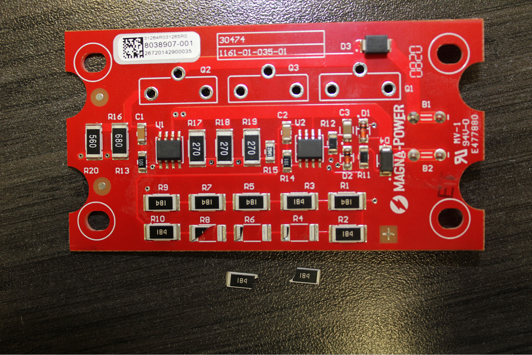
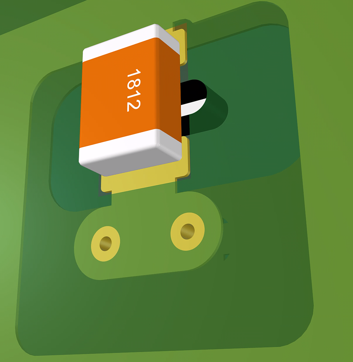
大多数Magna-Power PCB保持62 mil的厚度,这是行业中常见的叠层结构。对于大电流PCB,每层铜厚为5.6 mil,因此当需要多层时,会增加芯层厚度以保持最终组件的刚性。在4盎司、4层PCB上,Magna-Power的设计采用59 mil的介质芯层和92 mil的总板叠层厚度。芯层厚度可使电路板在贴片机上保持平整,从而实现更精确的元件放置,并防止波峰焊或回流焊炉中的热量导致翘曲。日常搬运、插入重型元件(变压器、散热器)造成的PCB弯曲可能导致表面贴装电阻和电容开裂。将元件放置在距离板边缘过近是一个常见的设计错误,在生产过程中会很快被发现;分板锯施加的压力会使PCB弯曲到足以使精密的MLCC电容器甚至厚膜电阻开裂,如图4所示。
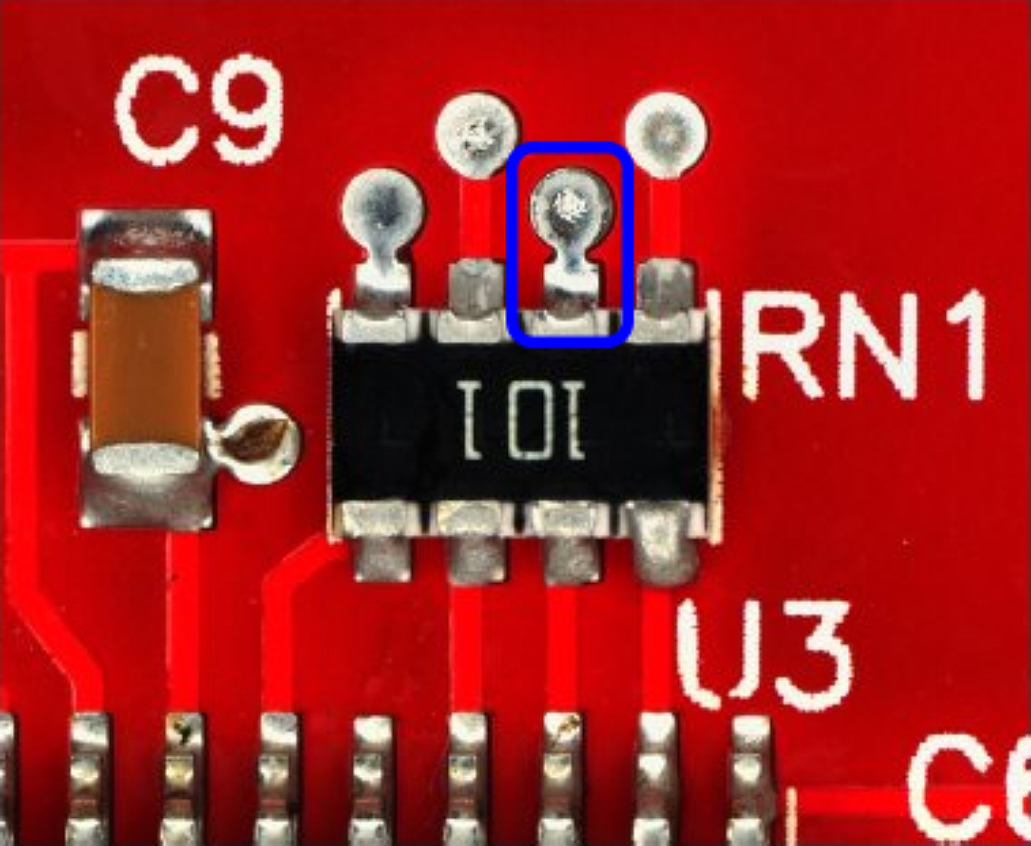
设计人员应充分了解PCB制造商的制造限制,这些限制会随铜厚规格而变化。一个关键且不易察觉的约束是最小阻焊间隙,它描述了阻焊油墨的印刷分辨率。例如,一家PCB制造商规定1盎司铜的最小阻焊间隙为8.5 mil,4盎司铜为11.5 mil。我们的长期供应商解释说,厚铜会使表面升高,在期望平整表面的阻焊工艺中造成问题。可能需要多次通过阻焊丝网印刷才能完全覆盖顶面并填充铜与介质之间的沟槽,这也增加了所需的公差。当间距过小时,PCB制造商通常会自动去除阻焊层,导致焊接缺陷。没有阻焊层时,同一网络上的焊盘会桥接在一起,如图5所示;过孔会将焊料从安装的芯片上吸走,使引脚缺少焊料,导致焊接缺陷[1],如图6所示。
高压印刷电路板
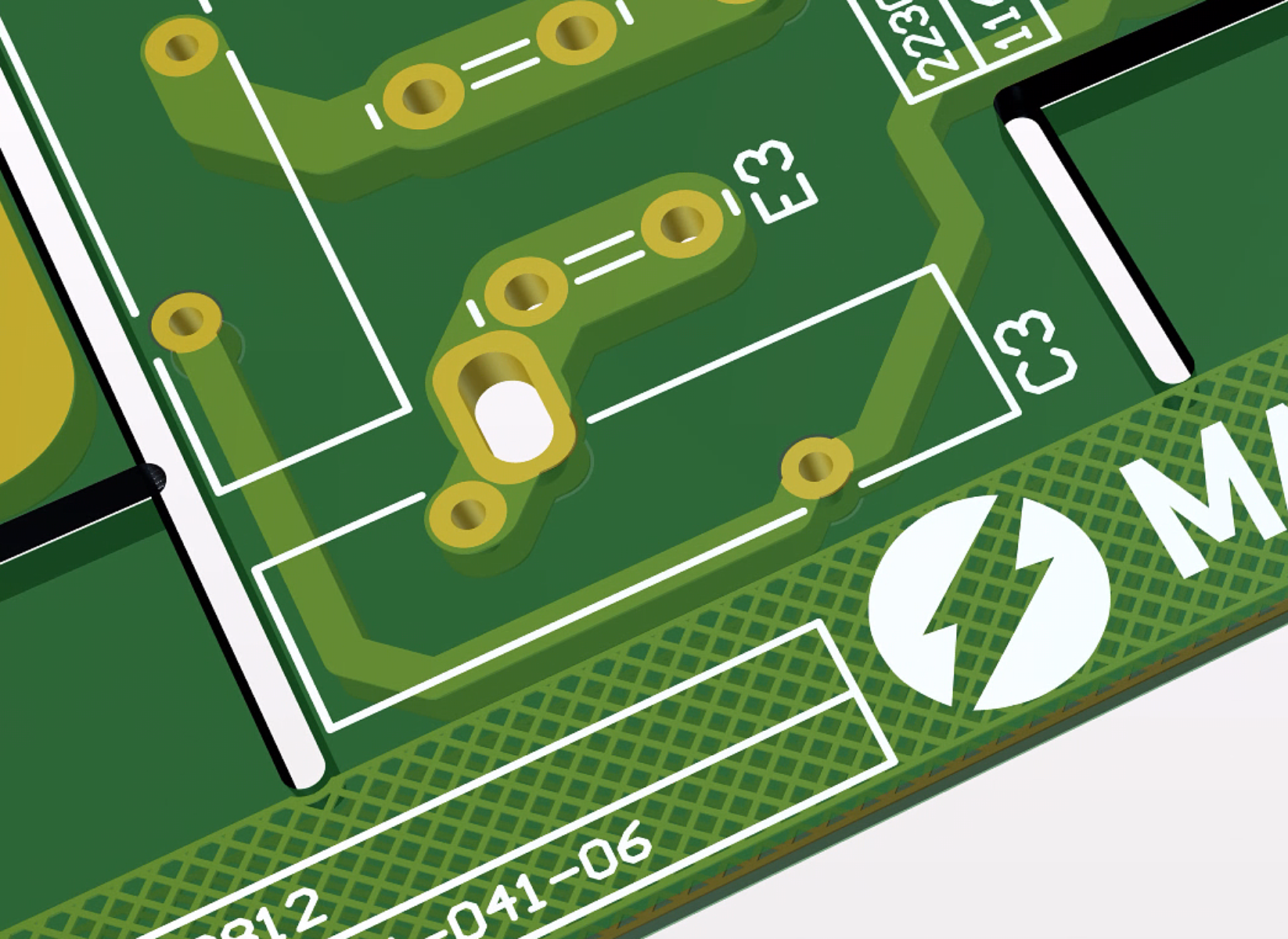
在大电流PCB设计中有许多与设备相关的约束需要考虑。而对于高压PCB设计,这些约束主要是电气方面的。在不同铜厚和制造商之间跟踪约束条件,如果手动完成将既繁琐又容易出错。Magna-Power广泛使用PCB设计软件中的设计规则来记录和即时自动执行复杂多样的约束。在PCB设计中发现的缺陷会被永久存储、版本化,并通过项目设计规则、通用设计规则库或主库元件封装来强制执行。通过这种方式存储缺陷,发现的问题可以在整个工程团队中共享,避免在未来项目中重复发生。高压PCB设计的两个主要设计规则是电气间隙和爬电距离。高电位和低电位的网络被识别和分组,并根据最恶劣的电压情况和IPC-2221 [2]中的建议设置它们之间的距离规则。基于规则设计的优势在于铜箔覆盖区域会自动调整以满足设计规则,同时在每个区域提供最大允许的铜面积。图7展示了我们高压输出组件上受约束布线的陶瓷电容器。在此示例中,爬电距离的优先级高于电气间隙,因此设计规则检查器会批准该设计,尽管其未通过电气间隙检查。此外,请注意电气间隙规则如何精确地在高电位区域切除铜箔。
所选的爬电距离还取决于所实施的生产工艺。IEC 60947-1 [3] 表明,表面污染物和介电材料会减小爬电距离,对于电源而言,这意味着更低的功率密度。如图7所示,在介电材料上铣削槽缝已在文献 [4] 中通过实验证明可将击穿电压提高20%。所有 Magna-Power 产品均为标准化、高精度的机架安装设备,在合理清洁的实验室环境(污染等级2)中运行,并据此进行设计。输入级的间距按1.2 kV最恶劣情况设计(480 V三相线路电源)。输出级间距由直流输出电压额定值决定。在极端情况下,如 Magna-Power 的 XR 系列电源(输出范围高达10 kVdc),输出部分的PCB在生产后全部进行清洗以防止电弧。大多数其他低压组件采用免清洗工艺,虽然减少了人工,但会残留助焊剂(污染物)。高压组件还应避免尖锐边缘,因为尖锐边缘可能成为电弧起弧点。可以通过在软件中执行锐角设计规则、使用圆角走线和铜箔填充,以及齐平剪切通孔元件引脚(如图8所示)来避免尖锐边缘。尽管采取了所有这些设计规则和生产预防措施,碎屑仍可能意外污染高压区域(例如,去毛刺不充分产生的金属碎屑)。因此,所有1 kV及以上的产品在进行任何出厂测试之前都要进行耐压测试。

内部制造的原型管理
在 Magna-Power,将原型与生产工单一起有效跟踪和管理一直是一项长期挑战,在业务逻辑和记录保存方面经历了多次迭代。目标是将原型工作视为任何标准工作,并让其遵循标准生产流程。让新设计经历尽可能多的工序将揭示电气和制造缺陷,这是内部生产的关键优势。建立小批量生产/原型运行需要一些前期记录工作:所有元件必须录入数据库,完成物料清单(BOM),签署采购订单,发出工单(WO),并完成配套。发现记录错误虽然不起眼,但同样重要。等到大规模生产时才发现这些错误可能会造成代价高昂的失误。本节描述了 Magna-Power 在制造部门读取设计所需的记录保存和版本管理方法,以及为支持记录录入和验证而开发的定制软件工具,最后是生产后的工程回顾——所有这些都将昂贵的设计迭代降至最低。
文档控制
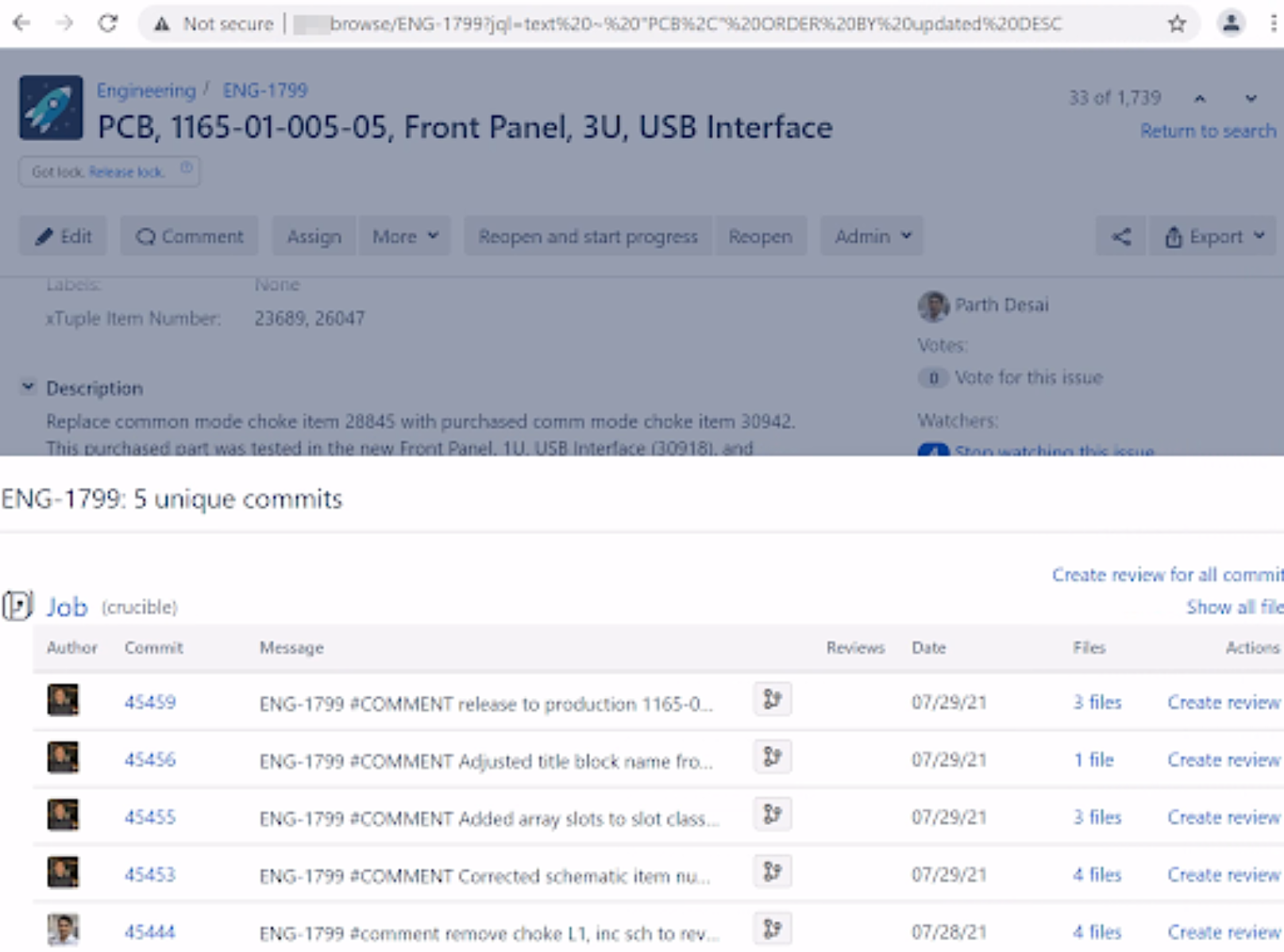
大多数生产部门依靠工程图纸将设计变为现实。新图纸和修改源于产品中的功能需求、问题或改进;由生产、管理、销售/市场或客户以工单形式提出。被分配此工单的工程师将研究并将相关工单分组,以便在同一原型运行中解决/推进多个工单。当图纸首次创建或修改时,它们会被提交到文件版本控制系统的工作文件夹中。每个更改都链接回原始工单,在同一位置提供完整的文件更改历史记录及其理由,如图9所示。在版本控制系统中,没有文件会被删除,只有授权人员才能查看或修改文件,每个人都有集中访问权限,并且两个工程师不能相互覆盖对方的工作。在高度协作的工程/制造环境中工作时,这样的系统是必需的。相同的版本控制用于原理图、布局、机械图纸、磁性元件图纸和源代码。该系统甚至用于存储复杂的贴片机配方和机器人程序,以便快速调用工作并确保可重复性。公司实施的工单/版本控制系统解决了工程和生产两个领域之间的重大文化冲突。工程师追求变革和改进,而制造商追求质量和可重复性。工单为生产提供了变更的合理性依据,而版本控制则锁定设计并确保可重复性。
生产记录
负责初始文档设计的工程师也是首先为元件和BOM创建新记录的人员。将工程、制造和计划明确分离的公司通常最终会出现不同步且容易出错的重复记录系统。Magna-Power 的垂直整合及其集中化记录使设计工具和制造设备之间能够共享数据,其优势将在本节中讨论。
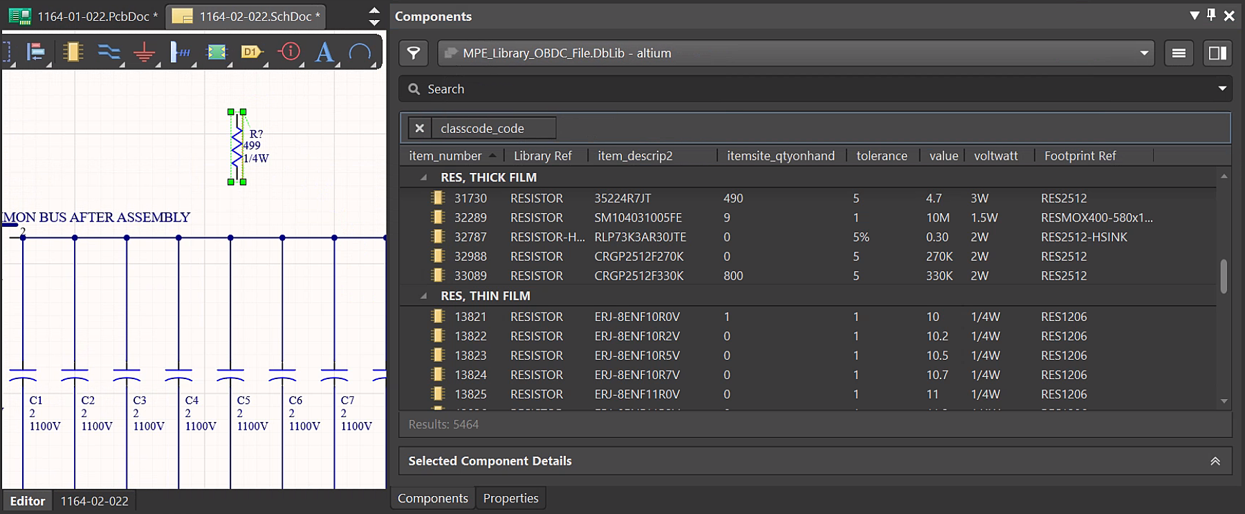
工程师在录入新元件时可以采取的最重要的记录策略就是尽量避免录入新元件。工程师应使用供应链中的现有元件,只有在确实必要时才引入新元件。那个1%的电阻真的需要吗,还是库房中现有的5%电阻就足够了?在审核供应商、验证授权分销商、协商价格、设置再订货水平和库存控制记录方面需要付出大量努力。在制造方面,贴片机的供料槽位有限。元件整合可以减少料盘更换,从而减少人工,并且减少搬运也降低了拣料出错的可能性。为了鼓励在新设计中重用物料,Magna-Power 将其中央数据库集成到其原理图和布局软件中。在原理图设计中,只显示在用元件及实时库存水平,如图10所示。将元件拖入原理图即可添加封装、符号和大约十个相关属性——其简便性鼓励了现有元件的重用。定制软件被开发用于从原理图提取数据并注入回数据库。对于复杂电路板,如公司新一代数字控制板(包含400多个元件),BOM只需一键即可注入企业资源计划软件。
随着设计的成熟,工程部门可能会进行调整以修复问题或实现功能,计划部门也可能在元件过时或难以采购时进行替换。在这些情况下,人为错误不可避免;工程部门可能忘记更新BOM,计划部门可能忘记通知工程部门修改原理图。此类错误导致设计文档与BOM不同步,生产部门困惑于哪个是正确的。为防范此问题,开发了定制软件,在PCB部门为贴片机创建配方时运行。该软件将BOM与原理图/布局进行比较并记录差异。该软件交叉引用标识符(如R1、C43等)、零件编号、元件属性(数值、电压、功率、公差),作为投入生产前的最终合理性检查。元件属性交叉引用至关重要,因为贴片机会将加载的属性与物理测量的电阻和电容进行交叉比对,以验证正确的料盘是否安装在了正确的供料位置上。
记录版本管理在发布至制造(RTM)后的几个关键节点进行。Magna-Power 会在首件检验(FAI)之后锁定文档的修订版(标签),此后不再允许更改。例如,PCB布局在从板厂返回后进行标签化,因为工程师在释放设计文件后通常会为制造商进行修正。类似的理念也适用于BOM的激活。当完成的组件通过测试后,设计工程师进行回顾审查。该工程师将审查所有生产工单上的反馈,以便做出知情决策。如果原型运行不顺利,工程师可以选择停用待定修订版,保留现有版本,并在新的待定修订版上重新尝试。这需要谨慎考虑,因为激活BOM或PCB即意味着批准进行大规模生产和大批量物料采购。
工单系统在经过多个工序和部门时提供了清晰的文档追踪链。回顾审查在关闭工单前为工程师提供了时间来审查和验证问题是否确实得到解决、识别改进领域,并为下一个设计周期生成新工单。该工作流程的成功很大程度上取决于各部门通过工单报告问题的勤勉程度以及工程师对生产过程的积极参与。
固件和软件版本控制
Magna-Power 上述的硬件工作流程、版本管理和工具借鉴了软件开发中更常见的做法。软件开发人员早已解决了多人协作管理多个数字文件的问题。这些开发人员还学会了将大型程序拆分为更小的组件,对稳定版本进行构建、验证和标签/版本管理。当这些实践应用于整个电子产品时,其复杂程度更上一层。
Magna-Power 最新的数字平台拥有独立的固件和引导加载程序代码库(包含五种不同的处理器和十个代码项目)、用于计算机控制的程序、自动化测试、LabVIEW驱动程序,甚至文档。复杂性的根源在于软件项目之间以及软件与硬件之间存在依赖关系。软件和硬件都在持续改进以满足客户需求。这种持续改进所产生的复杂性示例包括:
- 最新版本BOM需要特定版本的PCB;
- 新固件功能可能仅适用于特定范围的BOM版本;
- 处理器之间只有在相同固件版本下才能通信;
- 计算机只有在使用相同通信协议版本时才能与固件通信;
- EEPROM中的持久存储必须随着功能设置的添加、修改和删除而适应固件变更。
Magna-Power 选择通过一套复杂的、定制开发的持续集成服务器(CIS)来应对这些复杂性,该服务器旨在检测代码更改,然后编译、测试、加密、打包、标签和部署软件——既面向内部,也面向客户。CIS将这种日益增长的复杂性隐藏在工程和生产之外,使员工能够将精力集中在开发/生产上,而不是向前/向后兼容性或工具链问题上。这个CIS服务器与基于状态的模型设计相结合,使单一固件开发能够适用于电源、电子负载和其他特殊应用产品,同时允许客户随时通过互联网升级固件。作为替换件发送的电路板会自动从主板上的文件进行刷新升级,产品间连接(主/从)可以触发跨产品固件更新;迄今为止,多达三十七个处理器组成网络并升级了各自的固件。
电子与机械集成
一个电子组件可以由多个PCB组件、金属组件(支架和嵌件)、塑料零件、橡胶零件和磁性元件组成。组件的设计和制造涉及多个工程团队和制造部门。垂直整合提供了大幅缩短原型周期和快速沟通变更的灵活性,使制造问题在周期中期即可被发现,从而提高了产品的整体质量。
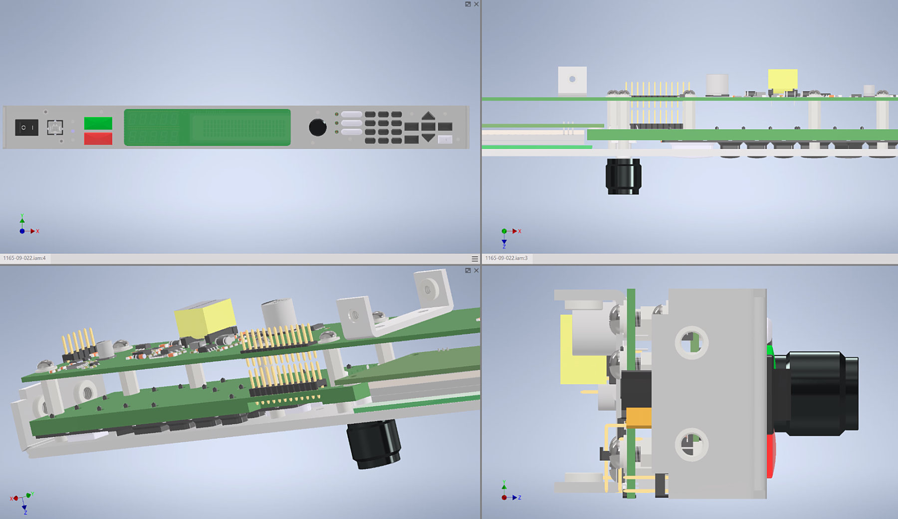
参数化建模是 Magna-Power 最新采用的工具,用于在实际构建之前检查电子组件的机械装配适配性。每个原型周期在时间、材料、工装和机会成本方面都代价高昂——因此在每次迭代中尽可能多地做到正确的动力十分强烈。参数化建模的一个有效案例是 Magna-Power 的新一代数字前面板,如图11所示。该设计需要在4.4 cm的垂直高度内层叠多块PCB,以安装VFD显示屏、键盘、导光管、旋转编码器和十个七段LED。电子、固件和金属部分由多个内部团队设计,键盘、Lexan和印刷垫则有外部合作方参与。在此设计中,电气团队为所有元件定义了3D实体,以便将精确的3D表示导入建模软件。机械团队利用PCB确定电路板安装位置、添加支架并为橡胶键盘创建开口。电气团队获得了一张正面面板图纸,将其导入电路板布局软件以锁定碳垫的接触位置。这种反复交互的过程说明了团队之间的沟通需求以及软件之间的数据交换需求。在此项目中,大多数设计缺陷在进入生产之前就被发现。仍有一些缺陷通过了检查,例如忽略了键盘开口处粉末涂层的厚度。然而,由于公司自有冲压机和粉末涂装系统,可以快速修正,使意外缺陷更容易管理。该项目的主要瓶颈是唯一外包的部件:键盘。
结论
设计一致性是贯穿 Magna-Power 历史的核心原则。随着工程师经验的积累,这种一致性成为直觉。这种灵活性对公司的成功至关重要,使其能够以相对较小的团队支持极其广泛的产品线。虽然设计一致性始终如一,但实现这一原则的策略已经(并将继续)随着公司的发展而演变。本文展示了基于软件的工具,这些工具在设计过程中实施约束、共享元件和规则库、验证原型工作流程,并自动执行生产记录与设计文件的核对检查。设计还必须考虑工艺、设备限制和标准,正如通过 Magna-Power 与众多PCB供应商合作的经验所描述的那样,其中详细说明了公司自身的内部生产工艺和几项关键的PCB设计策略。
关于作者
Grant Pitel ([email protected]) 是 Magna-Power Electronics 的首席技术官,公司位于美国新泽西州弗莱明顿。他在美国伊利诺伊大学厄巴纳-香槟分校获得电气与计算机工程硕士和博士学位。
Adam Pitel ([email protected]) 是 Magna-Power Electronics 的首席执行官,公司位于美国新泽西州弗莱明顿。他在美国新泽西州普林斯顿大学获得工程硕士学位。
参考文献
[1] "IPC-2221B", Generic Standard for Printed Board Design, November 2012.
[2] "IPC-A-610H", Acceptability of Electronic Assemblies, September 2020.
[3] "IEC 60947-1:2020", Low-voltage switchgear and control gear - Part 1: General rules, April 2020.
[4] J. Maxwell and E. Lemus, "Arc Season and Board Design Observations" presented at the Capacitor and Resistor Technology Symposium, Orlando, FL, USA, 2006.